Download
1 / 58
580 likes | 769 Views
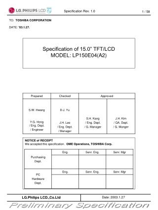
TO: TOSHIBA CORPORATION DATE: ’03.1.27. Specification of 15.0” TFT/LCD MODEL: LP150E04(A2). NOTICE of RECEIPT We accepted this specification. OME Operations, TOSHIBA Corp. - CONTENTS - Record of Revision --------------------------------------------------------------- 3

E N D
TO: TOSHIBA CORPORATION DATE: ’03.1.27. Specification of 15.0” TFT/LCD MODEL: LP150E04(A2) NOTICE of RECEIPT We accepted this specification. OME Operations, TOSHIBA Corp.
- CONTENTS - Record of Revision --------------------------------------------------------------- 3 1. Scope --------------------------------------------------------------- 4 2. General Specifications --------------------------------------------------------------- 4 2.1. Features 2.2.Dimensional Outline 3. Absolute Maximum Ratings --------------------------------------------------------------- 9 3.1. Absolute Ratings of Environment 3.2. Electrical Absolute Maximum 3.3. Mechanical ratings 3.4. The others 4. Optical Characteristics --------------------------------------------------------------- 16 4.1 Test Conditions 4.2 Optical Specifications 5. Electrical Characteristics --------------------------------------------------------------- 21 5.1. TFT LCD module 5.2. Backlight Unit 5.3. Regulation 6.Block Diagram --------------------------------------------------------------- 27 7. Input Terminal Pin Assignment --------------------------------------------------------------- 28 7.1 TFT LCD module 7.2 Backlight Unit 7.3 LVDS Transmitter 7.4Input Signal, Basic Display Colors and Gray Scale of Each Colors 8. Interface timing --------------------------------------------------------------- 35 8.1 Timing Parameters 8.2 Timing diagrams 8.3Power On / Off Sequence 9. Cosmetic Specification --------------------------------------------------------------- 38 9.1 Sampling 9.2 Conditions of Inspections 9.3 Defect modes 9.4 Mechanical inspection 9.5 Visual Inspection 9.6Electrical inspection 10. Packing --------------------------------------------------------------- 42 11. Labels--------------------------------------------------------------- 44 11.1 Labels 11.2 Others 11.3 Instruction of changing the Lamp parts - Lamp Ass’y Exchange process Defect modes 12. General Precaution --------------------------------------------------------------- 56 Appendix --------------------------------------------------------------- 58
1 2 1399 1400 R G B R G B R G B R G B 1 R G B : Pixel R G B R G B R G B R G B 2 R G B : Sub-pixel R G B R G B R G B R G B 1049 R G B R G B R G B R G B 1050 217.5um 217.5um 1. Scope This specification is applicable to LCD manufacturer’s 38.1cm (15.0”) diagonal size TFT-LCD module "LP150E04(A2)" designed for Personal Computer. 2. General Specification 2.1. Features Note 1)
2.2. Dimensional Outline ( Front figure )
90% 80% 60% 60 50 Wet Bulb Temperature [C] Storage Humidity[(%)RH] 40% 40 Operation 30 20 20% 10 0 10% -20 0 10 60 70 80 Dry Bulb Temperature [℃] 20 30 40 50 3. Absolute Maximum Ratings 3.1. Absolute Ratings of Environment Note 1) Temperature and relative humidity range are shown in the figure below. Wet bulb temperature should be 39C Max, and no condensation of water. Note 2) The surface temperature caused by self heat radiation of cell itself is specified on this item.
3.2. Electrical Absolute Maximum (1) TFT LCD Module (2) Back Light Unit
3.3. Mechanical Ratings Definitions of failure for judgment shall be as follows: (1) Function of the module should be maintained. (2) Current consumption should be smaller than the specified value. (3) Appearance and display quality should not have distinguished degradation. (4) Luminance should be larger than the minimum value specified in optical specification.
:COMPRESSION POINT Flat plate LCD [ Fig 1-1 ] :COMPRESSION POINT ABS natural 2.0t LCD Flat plate [ Fig 1-2 ] Note 1) (1) The compression condition of front side (a) Compression point : 12 points ( refer to Fig 1-1) (b) Compression condition: 20kgf, 3 sec, Tool diameter: 16 mm in diameter (refer to Fig 1-3) (2) The compression condition of rear side (a) Compression point : 21 points ( refer to Fig 1-2 ) (b) Compression condition : 30kgf, 3 sec, Tool radius: 30 mm in diameter ( refer to Fig 1-3)
10mm in diameter 10 16 B 1.5 A Rubber sheet [ Fig 1-3 ] (3) Dimension of the compression jig (a) compression jig for front side A = 16 mm in diameter B = 16 mm in diameter (b) compression jig for rear side A = 30 mm in diameter B = 28 mm in diameter
Z Y X Note 2) LCD fixing condition for z direction.
3.4. The Others (1) Static electricity pressure resistance (2) Sound noise There should be no uncomfortable noise. Being used under whatever surrounds, when power on/off, the panel should not generate uncomfortable noise. And regarding specified values are negotiated if it is needed. (3) Open / Short No smoke, no fiery at any open/ short test (4) MTBF : 50,000 Hr (except for backlight lamp)
4. Optical Characteristics 4.1. Test Conditions Ambient Temperature : Ta 25 5 C Ambient Humidity : Ha 65 20 %RH Supply Voltage : VCC =3.3V Input Signal : According to typical value in "Electrical Characteristics" FL Input Current : IL = 6.0mARMS FL Driving Frequency : fLF = 605 kHz FL Inverter : LG Inverter (6632Z-1301A) The measuring method is shown in 4.2. The following items are measured under stable conditions. The optical characteristics should be measured in a dark room ( Screen illuminance < 2lx ) or equivalent state with the methods shown in Note (6). 4.2. Optical Specifications
* Gray scale specifications. ( Gamma Value = 2.2 ) Note 1) Definition of viewing angle and Note 2) LCD fixing condition for z direction. The contrast ratio can be calculated by the following expression. Contrast Ratio (CR) = L63 / L0 L63 : Luminance on the white raster (gray scale level L63) L 0 : Luminance on the black raster (gray scale level L0)
Toff Ton % 100 90 Optical Response 10 0 Bright Bright Dark VIEW AREA VIEW AREA (0, 0) (0, 0) (100, 100) YA(680, 310) YA(680, 310) (350, 480) Gray Level 0 (1399, 1049) (1399, 1049) Gray Level 42 Gray Level 42 Note 3) Definition of response time Note 4) Definition of surface luminance of white Measure the luminance of white at Center point. Surface luminance of white YL Note 5) Definition of Cross Modulation (DSHA) DSHA = | YB – YA | / YA100 (%) Where: YA = Luminance of measured location without darkest gray pattern (cd/m2) YB = Luminance of measured location with darkest gray pattern (cd/m2)
Light Shield Room ( Screen illuminance < 2lx) LCD module LCD panel Center of the screen ( Field of view = 1 deg) Photometer (Prichard 880 or equivalent) 500 mm Horizontal Line number [pixel] 0 349 699 1049 1399 1336 62 Vertical Line number [pixel] 0 62 7 8 6 : test point 262 2 3 9 1 524 10 787 5 4 11 12 13 987 1049 Active area Note 6) Measuring setup The measurement suppose to be executed after stabilized the panel at given temperature during 30min. The measurement shall be executed 30 minutes after lighting at rating. The luminance of white should be typical luminance ( Typical Condition IL=6.0mA ). In order to stable the luminance, LCD shall not be got winds. Note 7) Definition of 13 points white variation W, CR variation CR and average luminanceYL W = Maximum luminance of 13 points / Minimum luminance of 13 points CR = Maximum CR 13 points / Minimum CR of 13 points YL = Luminance of 5 points(1~5) / 5
2.14mm 17.5mm 11.6mm 2.14mm 10.9mm 12 17.5mm Active area 16 Measuring Spot 500 mm 17.5 2deg. D(x+1,y-1) L(x+1,y-1) L(x-1,y-1) L(x,y) L(x+1,y+1) Note 8) Definition of White Variation dL : measure the luminance of white at 13 11 points. dL = [ | L(x,y) – L(x+i, y+j) | / ( L(x,y) D(x+i, y+j) ) ] 100 (%/mm) where 2 x 15, 2 y 11, i = 1, j = 1
Active Area Display Brightest Gray scale Display Darkest Gray scale R G B Display Brightest Gray scale R G B R G B R G B R G B 5. Electrical Characteristics 5.1. TFT LCD module Note 1) Recommended LVDS transmitter :THC63LVDF823A, Thine. LVDS receiver included in this module is THC63LVDF824A. Note 2) Typical condition as follows. : fV= 60Hz, fCLK = 54 MHz, VCC= 3.3V. Note 3) Power dissipation check pattern. (a) White pattern (b) Mosaic pattern (C) Max. pattern Display Darkest Gray scale
VCC rising time is 470us 3.3V 0.9 VCC 0.1 VCC GND Note 4) Measuring condition of rush current.
VL: High Voltage Line FL Inverter A A TFT LCD Module ~ ~ GL: Low Voltage Line : AC ampere meter 5.2. Backlignt Unit Note 1) Lamp current is measured with a high frequency current as shown below. Note 2) Refre to IL X VL to calculate. Note 3) Life time of Lamp can be defined as the time in which it continues to operate under the condition T = 25C 2C and IL= 6.0 mArms until one of the following events occurs. 1. When the brightness becomes 50% or lower than it’s original. 2. When the Effective ignition length becomes 80% or lower than it’s original value. ( Effective ignition length is defined as an area that has less than 70% brightness compared to the brightness in the center point.) Note 4) The discharge shall be connected uniformly. Slide up method shall be used for voltage application. Above voltage is applied voltage to both ends of the lamp as the starting voltage. ( Above value is not output voltage of inverter.) Note 5) The lamp shall be lighted stably. Slide up method shall be used for voltage application. Above voltage is applied voltage to both ends of the lamp as the established starting voltage. (Above value is not output voltage of inverter)
* Asymmetry rate: | I p – I –p | / Irms * 100% * Distortion rate I p (or I –p) / Irms I p I -p ***Requirements for a system inverter design, which is intended to have a better display performance, a better power efficiency and a more reliable lamp, are following. It shall help increase the lamp lifetime and reduce leakage current. a. The asymmetry rate of the inverter waveform should be less than 10%. b. The distortion rate of the waveform should be within √2 ±10%. * Inverter output waveform had better be more similar to ideal sine wave.
Note 5) Detail description of creepage distance [ Section ‘A’ ]
5.3. Regulation The set (which LCD module is assembled into) should conform to the regulations below. (1) EMI Regulations. CISPR : Pub.22 CLASS B FCC : PART15 CLASS B VCCI : CLASS B (2) Safety Regulations (Only LCD) IEC 950 UL 1950 (3) Material list concerning
6. Block Diagram Lamp: -SS20D3065N6580C2882600S 1. Hot (Pink) 2. Cold (Blue)
1 30 7. Input Terminal Pin Assignment 7.1. TFT LCD module Note 1) Recommended LVDS transmitter :THC63LVDF823A, Thine. LVDS receiver included in this module is THC63LVDF824A, Thine. 7.2. Backlight Unit Using Connector : BHTR-02VS (Maker : JST) (Contact Pin of VL : SBHT-002T-P0.5(Maker :JST )) (Contact Pin of GL : SBHT-002T-P0.5(Maker :JST ))
7.3. LVDS Transmitter 7.3.1. Pin Description : THC63LVDF823A, Thine.
7.3.2. Switching Characteristic [VCC = 3.0 ~ 3.6V, Ta = -10 ~ +70℃]
7.3.3. AC Timing Diagrams (1) TTL Input (2) LVDS Output (3) TTL Intputs (4) Phase Lock Loop Set Time
7.4. Input Signal, Basic Display Colors and Gray Scale of each Color Note 1) 0: Low level voltage, 1: High level voltage
8. Interface Timing 8.1. Timing Parameters This is the signal timing required at the input of the LVDS Transmitter. All of the interface signal timing should be satisfied with the following specifications for its proper operation.
Power supply for LCD (VCC) Interface Signal (Tx) Power for Lamp 8.3. Power On/Off Sequence Note 1) Please avoid floating state of interface signal at invalid period. Note 2) When the interface signal is invalid, be sure to pull down the power supply for LCD VCC to 0V. Note 3) Lamp power must be turn on after power supply for LCD and interface signal are valid.
9. Cosmetic Specification 9.1. Sampling A.Q.L (Acceptable Quality Level ): MIL-STD, 105E Level II, Major: 0.65 , Minor: 1.5 9.2. Conditions of Inspections (1) Ambient Temperature : 255C (2) Ambient Humidity : 6520%RH (3) Illumination : 200 – 500 Lux ( nominal 350 Lux ) under the fluorescent lamp (4) Viewing Distance : Approximately 30cm by the eyes of the inspector from the module (5) Viewing angle :The surface of the module and the inspector’s line shall be at 90 45 degrees. (6) Display pattern : Pure Red, Green, Blue, Black, White, Gray level 0 - 63 9.3. Defect modes 9.4. Mechanical Inspection (1) Light leakage: No light leakage between metal chassis (bezel) and glass (2) No sharp edge (3) The mounting holes: No Changed (Side fixed type) (4) PCB Appearance: No pattern peeling snapping / No electrically short If there are repair portions,the repair portions on PCB is covered by epoxy resign (5) Soldering: No cold solder joint, lead move when pulled (6) Bezel, Frame, Connectors: No distinct stain, rust or scratch, no pin bending
D D W W L L a b 9.5. Visual Inspection [ D : diameter, W : width, L : length, N : count ] Note 1) Inspection area should be within bezel opening. Note 2) Dusts which are bigger not less than 0.10mm (0.1W) shall be judged by "Average Diameter". Note 3) Scratches which are bigger not less than 0.05mm (0.05W) shall be judged by "Average Diameter". Average Diameter D = (a+b)/2 (mm)
RGBRGBRG RGBRGBRG RGBRGBRG Quantity of LCD Average dot defect NAVE < 1 0 1 2 3 4 5 6 7 8 Count of dot defect in a LCD Required distribution of dot defect 9.6. Electrical Inspection (1) Dot defect a) Inspection patterns for dot defect are Pure Red, Green, Blue, Black, and White. b) Adjacent two dots will be counted as two dots. c) The distribution of dot defects should be below. Average value of dot defect s should be less than 1. d) The definition of 2 adjacent dots.
(2) Light leakage Light leakage can not be seen between metal chassis (bezel) and glass when displaying black plane. (3) Image sticking Image sticking pattern shall not be to persist longer than 1second after displaying following pattern 8 hours in the room temperature condition. (4) Glue/stain/dirt Glue, non-removable stain and dirt which are visible in the inspection area are not acceptable.
10. Packing (1) Packing Form Corrugated cardboard box and EPPas shock absorber. (2) Packing Method Packing Material Packing Weight: 265g (1BOX/10Module)
2 sides( LABEL Position) (3) Packing Specification (4) Package Label Package label should be at least shown the following information. a) TOSHIBA code name(G33C0000R110) which will be numbered by Toshiba b) Revision number which be numbered by LCD maker c) Quantity d) LCD maker e) Model number which be numbered by LCD maker f) Production Year / Month (5) Location of Package label : 2 points ( Side ) LP150E04 [G33C0000R110] A2
A B C D E F G H I J K L M 11. Labels 11.1. Labels. (1) LCD code Label on LCD LCD code label should be at least shown the following information. (a) TOSHIBA code name (G33C0000R110) which will be numbered by Toshiba & Bar code (Bar code : CODE-39 High-density ) (b) LGPL Serial number CODE ( numbered by LCD maker , less than equal 13 digits) A, B ,C : Size D : Year E : Month F,G : Panel Code H : Assembly Code I,J,K,L,M : Serial No. Note 1) Year Note 2) Month Note 3) Serial No. Serial NO. Is printed on the label. The label is attached to the backside of the LCD module. This is subject to change without prior notice. - Bar code of Serial number - Revision number (numbered by LCD maker) - Bar code of Revision number - LCD maker - LCD Model number ( numbered by LCD maker) - Production Year / Month
Example > LABEL : 72mm X 30mm TOSHIBA CODE 39 High-density LGPL Serial Number Code 128 High-density (2) Caution Texture and Labels on LCD [Disposal of CCFL] [High Voltage]
(3) Label Locations on LCD 11.2. Others (1) Backlight repair parts kit : 6913L-0139A(G33C0000R110001)
LP150E04 [G33C000R110001] A2 [6913L-0139A] (2) Package specification of Backlight repair parts kit a) Individual packing b) Master carton Packing method c) Label
11.3. Instruction of changing the Lamp parts - Lamp Ass’y Exchange process 11.3.1. Disassembly of outside tape / Cover shield (1) ① Disassembly of Tape adhesive used for B/L Wire fixing Caution: Pressure or stress should not be given on B/L Wire. (2) ② Disassembly of Cover shield(G) Caution: Pressure or stress should not be given on Gate TCP. (3) ③ Disassembly of Cover shield(C) Caution: Pressure or stress should not be given on Source PCB. Usage of gloves with anti-electric discharge coating is recommended. To eliminate possible damage on circuits occurred by ESC. (4) ④,⑤ Disassembly of Tape shield and Tape Adhesive used for Top case fixing Caution: Pressure or stress should not be given on Top case during this process
11.3.2. Disassembly of Top case (1) ① Disassembly of Top Case Caution: Pressure or stress should not be given on Top Case and Gate TCP.
11.3.3. Disassembly of Source PCB and Gate PCB (1) ① Disassembly of Source PCB. Caution: Pressure or stress should not be given on PCB and TCP during removing double tape. (2) ② Disassembly of Gate PCB. Caution: Pressure or stress should not be given on PCB and TCP during removing double tape.