MRS Fall 2008
Multiple Exciton Generation in CNT *N1.1 Multiple Exciton Generation in Colloidal Semiconductor Nanocrystals for Enhanced Solar Energy Conversion N1.2 Charge Carrier Multiplication and Nature of Excited States in PbSe Quantum Dots

MRS Fall 2008
E N D
Presentation Transcript
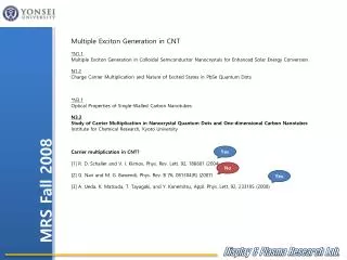
Multiple Exciton Generation in CNT *N1.1Multiple Exciton Generation in Colloidal Semiconductor Nanocrystals for Enhanced Solar Energy Conversion N1.2Charge Carrier Multiplication and Nature of Excited States in PbSe Quantum Dots *N3.1Optical Properties of Single-Walled Carbon Nanotubes N3.2Study of Carrier Multiplication in Nanocrystal Quantum Dots and One-dimensional Carbon Nanotubes Institute for Chemical Research, Kyoto University Carrier multiplication in CNT? [1] R. D. Schaller and V. I. Klimov, Phys. Rev. Lett. 92, 186601 (2004) [2] G. Nair and M. G. Bawendi, Phys. Rev. B 76, 081304(R) (2007) [3] A. Ueda, K. Matsuda, T. Tayagaki, and Y. Kanemitsu, Appl. Phys. Lett. 92, 233105 (2008) MRS Fall 2008 Yes No Yes
Bulk intermediate band solar cells • *N5.1Open Questions in the Implementation of the Intermediate Band (IB) Solar Cell • Instituto de Energia Solar, Universidad Politecnica de Madrid, Madrid, Spain • QD IBSC problems • Too small sub-band-gap current is obtained because of the low density of QDs (limited to about 1E17 per cm3) as consequence of their large size. • Not too many QD layers can be grown without spoiling by stress the solar cell performance. • The voltage is reduced by the quantum well associated to the wetting layer that is formed at the time that the QDs are grown and also by the QD levels that appear closely spaced near the valence (VB) and conduction (CB) bands • Bulk IBSC • Problem) • Deep levels in the semiconductor band gap are known to be the origin of non-radiative recombination • Solution) • Mott transition is reached, the non-radiative recombination disappears • Current materials) • Zn-Mg-Te-O alloys - O ion implantation & pulsed laser melting • Ga-As-P-N alloys - N ion implantation. • V-In-S compounds - Solvo-thermal synthesis • Proposal) • Ti and Fe are found to be good candidates to form an IB material in CuGaS2 MRS Fall 2008
Intermediate band & Up-Down Conversion : Molecular Approach Molecules over Rare-earth doped solid High quantum efficiency Process is scalable Dye-sensitized solar cell application *N6.1Up-Conversion in Multi-component Organic Systems: Enhancement of the Local Spectral Power Density of the Terrestrial Solar Irradiation? Max Planck Institute for Polymer Research, Mainz, Germany Sony Deutschland GmbH, Materials Science Laboratory *N6.4A Molecular Approach to the Intermediate Band Solar Cell School of Chemistry, University of Sydney Blackett Laboratory, Imperial College, London MRS Fall 2008
QD 3D Periodic Array *F1.1Self-organization and Chemical Doping in Solution Processed Semiconductor NanocrystalSuperlattices Chemistry and Materials Science & Eng, University of Pennsylvania F1.2Binary Superlattices of PbSe and CdSeNanocrystals Debye Institute for NanoMaterials Science, University of Utrecht, Utrecht, Netherlands MRS Fall 2008 QD 3D Transport N1.4Sensing Charge Through Arrays of PbSeNanocrystals with a Narrow MOSFET N2.3Using a Nanometer Scale MOSFET as a Charge Sensor *N4.1The Use of Multi-Size Arrays of Colloidal Quantum Dots to Study Energy and Electron Transport in QD Junctions N4.2Temperature Dependent Characteristics of Thin Film Nanocrystal Solar Cells
Surface Treatment N2.2Schottky-Quantum Dot Photovoltaics for Efficient Infrared Power Conversion Electrical and Computer Engineering, University of Toronto Chemistry, Universite de Montreal, Montreal, Quebec, Canada N2.4Fourfold Efficiency Improvement in PbS Quantum Dot Photovoltaic Devices via Trap State Passivation by Ethanethiol Electrical and Computer Engineering, University of Toronto N14.15Surface Modification of CdSe Quantum Dots with RegioregularThiopheneOligomers for High Efficiency Hybrid Solar Cells GIST, Gwangju, South Korea. Thiophene MRS Fall 2008
Hot carrier solar cell *N11.1Tapping the Thermal Energy: is a Hot Carrier Solar Cell Possible? Approach periodic networks of quantum structures, such as semiconductor nanoparticles, incorporated into the absorber material can significantly reduce the scattering between phonon modes double barrier resonant tunnel structures with the resonant energy level provided by a single quantum dot layer whose size, uniformity, and density will be optimized against overall cell performancesize, uniformity, and density will be optimized against overall cell performance MRS Fall 2008
Solar Concentrator *N12.1Nanocrystal Doped Luminescent Solar Concentrators *N12.2High Efficiency Organic Solar Concentrators N12.3Reducing Re-absorption Losses in Luminescent Solar Concentrator with Nanorods MRS Fall 2008
Radial Solar Cell • N13.1Radial pn Junction Solar Cells, Past, Present, and Future. • California Institute of Technology, Pasadena, California • Chemistry, California Institute of Technology, Pasadena, California. • N13.2Single and Tandem Axial p-i-n Nanowire Photovoltaic Devices • Chemistry and Chemical Biology, Harvard University • Mechanical Engineering, Stanford University • School of Engineering and Applied Sciences, Harvard University • N13.4Characteristics of Radial p-n Junction Nanowire Solar Cells Grown • by Vapor-liquid-solid Technique • IBM Research, Yorktown Heights, New York. • F8.5Electrodeposition of NanostructuredZnO on Textile Electrodes • a New Starting Point Towards Flexible Low-Cost Photovoltaics • P5.2A Photovoltaic Textile Material Based on SiCMicrowires and • poly(3-alkylthiophenes) • University of Paderborn, Paderborn, Germany. • Knitted Solar cell? MRS Fall 2008
Radial Solar Cell N16.23D Dye-sensitized Solar Cells (Tandem cells) Prepared by Nano-interface Control- Improvement of Light Harvesting Properties and Electron Collection Properties- Kyushu Institute of Technology, Kitakyushu, Fukuoka, Japan Nippon Steel Chemical Co., Ltd., Kitakyushu, Japan Perfect sealing of electrolyte! MRS Fall 2008
Radial Solar Cell 11:30 AM N16.6High Efficiency Photosplitting of H2O using TiO2/TiSi2 Heterostructure Complex Nanomaterials Chemistry, Boston College, Chestnut hill, Massachusetts MRS Fall 2008
Solution-processed Inorganic Materials F2.9Solution Processed Silver Sulfide Filament Memories Electrical Engineering, UC Berkeley Sulfidizing in sulfur solution *F8.4Electrochemical Atomic Layer Deposition (ALD) The University of Georgia, Athens, Georgia A solution Empty solution B Solution MRS Fall 2008
Solution-processed Inorganic Materials F6.16Low-Temperature Plasma Processing Promoting Densification-Crystallization of Sol-gel Titanium Oxide Thin Films IMIP-CNR and INSTM, Department of Chemistry, Bari University, Bari, Italy ISTM-CNR and INSTM, Department of Chemistry, Padova University, Padova, Italy Department of Chemistry, Padova University, Padova, Italy F9.15Low Temperature Solution-Based Fabrications of Metal Oxide Semiconductor Films by Mechanical Sintering Organic Semiconductor Device Research Group, National Institute of Advanced Science and Technology, Tsukuba, Ibaraki, Japan 120℃ MRS Fall 2008 Sol-gel TiO2
Solution-processed Inorganic Materials F6.17Low Temperature Sintering of TitaniaNanoparticles Utilizing Hydrothermal Treatments Materials Science & Engineering, Rutgers, The State University of New Jersey F6.18Structural and Electrical Properties of Indium doped Single Crystal ZnO Films Synthesized by Hydrothermal Method IMRE-Singapore, Singapore TiO2 Sintering under 100℃ MRS Fall 2008
Solution-processed Inorganic Materials F2.4Nanoscale Zinc Oxide as Semiconductor Material in a Printed Field Effect Transistor Device TU Darmstadt, Darmstadt, Germany Merck, KGaA, Darmstadt, Germany Processing temperatures well below 200°C molecular precursor → naocrystallineZnO → self adhering films F2.7Rapid Electrical Sintering of NanoparticleStuctures VTT Sensors and Wireless Devices, VTT, Espoo, Finland MRS Fall 2008
Solution-processed Photovoltaic Materials *P6.1/F7.1FASST® Reactive Transfer Printing for Morphology and Structural Control of Liquid Precursor Based Inorganic Reactants National Renewable Energy Laboratory, Golden, Colorado Similar process to anodic bonding : Enables lower bonding temperature MRS Fall 2008
Solution-processed Photovoltaic Materials P6.2/F7.2Use of Direct Write Methods for Low Cost Photovoltaics National Renewable Energy Laboratory, Golden, Colorado Colorado School of Mines, Golden, Colorado Spray precursor solution into heated substrate Spray-deposited CIS film : Dense and continuous MRS Fall 2008
Solution-processed Photovoltaic Materials *P6.4/F7.4All-chemically Deposited Thin Film Solar Cells Centro de Investigacion en Energia, Universidad NacionalAutonoma de Mexico, Temixco, Morelos, Mexico By chemical bath deposition method CdS - 3h Sb2S3 - 6h PbS - 2h Efficiency ~ 1% *P6.5/F7.5Solution Routes to Synthesis of Cu(In,Ga)(S,Se)2 Chalcopyrite Solar Cells IRDEP, CNRS, Chatou, France. Electrodeposition MRS Fall 2008
New materials AM N15.4Tin Monosulfide as Light-Absorbing Material in Thin Film Photovoltaic Applications Energy and Mineral Engineering, The Pennsylvania State University, State College SnS Environmental friendliness Cheap cost of raw materials tin and sulfur High absorption coefficient (α >10^4 cm-1) Favorable band gap (1.1-1.4 eV, p-type) P5.4Rational Synthesis of Earth Abundant Materials for High Efficiency Heterojunction Thin Films Solar Cells Department of Mechanical Engineering, Massachusetts Institute of Technology, Cambridge, Massachusetts Laboratory for Manufacturing and Productivity, Massachusetts Institute of Technology, Cambridge, Massachusetts Department of Materials Science and Engineering, Massachusetts Institute of Technology, Cambridge, Massachusetts Cu2O MRS Fall 2008