Download
1 / 42
420 likes | 432 Views
Explore the WaveCatcher family of fast digitizers for precise signal measurements with a 5-ps precision at the system level. Learn how waveform digitization and sampling matrix structures can achieve high-resolution time measurements.

E N D
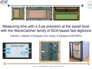
Measuring time with a 5-ps precision at the systel level with the WaveCatcher family of SCA-based fast digitizersD.Breton, J.Maalmi, P.Rusquart (LAL Orsay), E.Delagnes (CEA/IRFU)
Introduction The technologies have evolved at an amazing rate in the last decade, and during this period our electronics engineer everyday work has been transformed consequently Sometimes we have to design systems housing only few channels, for instance for our test or characterization benches, other times large scale systems for physics experiments, thus pushing us to look for the best solution to perform as precise as possible signal measurements at the lowest cost and power consumption Our consecutive developments thus made us use high-end commercial ADCs as well as developing high performance TDCs and analog memories Now we deal with many GS/s, which actually permits getting closer to ps => we can aim at measuring the time using waveform digitization …
Current most performant TDC use digital counters and Delay Line Loops (DLLs): => advantage: produces directly the encoded digital value => but the resolution is at least limited by the DLL step (often by environmental factors) Actual time resolution of today’s available most advanced ASICs: ~ 20 ps New developments are ongoing A few comments about TDCs BUT a TDC needs a digital input signal • analog input signal has to be translated to digital with a discriminator • additional jitter and residues of time walk effect enter the game • overall timing resolution is given by the quadratic sum of the discriminator and TDC timing resolutions
ADC and TDC Actually, the best way to precisely measure the arrival time of a signal is to digitize it with a very fast and precise ADC. Indeed, once data is digitized, one can perform a digital treatment of data to precisely extract time information Waveform contains all information (if properly digitized) Depending on the information requested (amplitude, charge, time, FFT, …), different types of algorithms can be used One of the goals is to find the both simplest and most effective algorithms which could be integrated within companion FPGAs Waveform sampling can be used for designing high performance TDCs It was shown that > 1GS/s sampling rate together with a good SNR (>10bits) was leading way to the ps level Caution: signal to noise ratio is always an issue, even for a TDC
Targetting the ps … • As said before, a perfect digitizer for fast signals would be for instance a 10-GS/s 12-bit flash ADC. • The 120Gbits/s output data rate per channel could make anybody nauseous, especially at large scale … • Moreover, 10 GS/s sampling doesn’t give enough time to process the sampled signal in real time • the idea to digitize only the interesting part of the signal rises! • storing the analog signal at high sampling rate and stopping the recording whenever something interesting occurs, just the time to digitize and transfer data to the next readout stage • This reduces the power and the dataflow by a huge factor • But … this induces dead-time for digitization • Depending on the application, dead-time can be more or less bothering …
Circular analog memories: basic principles An analog memory can record waveforms at very high sampling rate (>>GS/s) After trigger, they are digitized at much lower rate with an ADC (~10/20 MHz) • A write pulse is running along a folded delay line (DLL). • It drives the recording of signal into analog memory cells. • Sampling stops upon a trigger signal. • Readout can target an area of interest, which can • be only a subset of the whole channel • Dead time due to readout should remain as small • as possible (<100ns / sample).
Our favourite solution: a Sampling Matrix • We started designing analog memories in 1992 with the first prototype of the Switched Capacitor Array (SCA) for the ATLAS LARG calorimeter. 80,000 chips produced in 2002, now on duty on the LHC. • Since 2002, 3 new generations of fast samplers have been • designed (ARS, MATACQ, SAM): total of more than30,000 chips in use. HAMAC 1998-2002 Sampling at 3.2GS/s MATACQ 2000-2003 Readout 12 bits 10/20 MHz ADC Patented in 2001 SAM 2005 SAMLONG 2010-2012
Advantages/ Drawbacksof the Sampling MATRIX structure • Short DLL: • Smallest cumulative jitter. • Junction between DLL. • 1 servo control of Delay / Column => high stability. • Analog Input Buffering: • High input impedance: • Linearity • No DC input current • No Ringing. Flat response • Power consumption • BW limitation • Analog bus split in divisions: lines • Shortest analog bus : • More uniform bandwidth. • Less analog delay along the bus. • Parallel readout => faster readout. • 1 buffer / line : • Better analog BW/power consumption FOM • No ghost pulse or baseline shift effect at high signal rate • Offset between lines (corrected by DAC on-chip). • Initial philosophy: possibility to work with no off-chip correction (pedestal, amplitude, time) => limit external computing Analog design isfullydifferential
Analog memories vs ADCs Analog memories actually look like perfect candidates for high precision measurements at large scale: Like ADCs they catch the signal waveform TDC is built-in (position in the memory gives the time) Only the useful information is digitized (vs ADCs) => reduced dataflow and power Any type of digital post processing can be used Main design difficulty is less sampling frequency than signal bandwidth Their drawbacks: The limited recording depth The readout dead-time limiting the input rate But: Only a few samples/hit can be read => this may limit the dead time Simultaneous write/read operation is feasible, which may further reduce the dead time
Board and system developments • based on SAMLONG.
The USB_WaveCatcher board (V6) 2008/2010 The autonomous test bench The historical 2-Channel module
2011/2013 • The 16/18-channel board • 1.6mm thick • 10 layers • 233 x 220 mm² • 3200 components • 25 power supplies (5 global, 20 local) • Four 4-channel blocks (can be used as mezzanines on other boards) • 2 extra channels dedicated to « digital » signals
2-channel front-end diagram BACKPLANE Ch0 + Low Threshold - + High Threshold - Ch1 + ½ Front End FPGA (TimeStamp,Q,A) Low Threshold Trigger in - FPGA Controller + High Threshold - Trigger out Run, read Event data Ch0 SAMLONG (1024 samplingcells) clk 12-bit ADC Ch1 USB x 8
Front-end block can be used as a mezzanine The latter’s design is compatible with the CAEN X743 digitizerboardfamily 2013 2011 Front-end mezzanine LAL motherboard for 2 mezzanines 2012
Building largerscalesystems The controllerboard 2011/2012 64-channelbackplane • To synchronisemanyboardsa controllerboardisneeded, plus a backplane for the interconnections • we have built a very compact 64+8-channel system: • alreadyused for the CORTO Cosmic Ray Telescopeat Orsay and for a prototype of new Gamma Spectrometer for particle detection, soon at CERN for beam characterization • we are also building a 960-channel system based on 3 6U-crates (for the first module of the future SuperNemo neutrino experiment)
Present and future system features (not exhaustive) Possibility to add anindividual DC offset on eachchannel Individualtrigger discriminatoron eachchannel Integrated raw trigger rate counter on eachchannel External & internal trigger + different modes for coïncidence triggering 2 extra memorychannelsfor « digital » signals on 16-channelboard => canbeused as additionalanalog inputs One pulse generatoron each input Externalclockinput for multi-board applications (8, 16 & 64-channel) Embedded USB, UDP and Gigabit optical interfaces (8, 16 & 64-channel) Possibility to upgrade the firmware via US Embedded charge extraction Embedded signal amplitude and baselineextraction Embedded digital CFD for time measurement NEW
The 64-channel software Main panel: oscilloscope like, but 64 channels ! Vertical panel
The 64-channel software (2) Horizontal/acq panel Trigger panel
The 64-channel software (3) Noise statistics panel • Software also comprises a powerful time measurement panel
Board performances: examples Comparison oscilloscope/WaveCatcher
Summary of the WaveCatcher performances. • DC-coupled 1024-deep channels with 50-Ohm active input impedance • ±1.25V dynamic Range, with full range 16-bit individual tunable offsets • Bandwidth~ 500MHz • Signal/noise ratio: 11.7 bits rms (noise = 700 µV RMS) • Sampling Frequency: 400MS/s to 3.2GS/s • SAMLONG power consumption: ~400 mW for 2 channels (full bandwidth) • 2-channel readout dead-time for 1024 cells: 125 µs (66 µs @ 20 MHz) • Acquisition rate (full events) is not limited by USB (30 Mbytes/s) but by the software and the capacity to store events on disk • Acquisition rate (data extraction in FPGA): see next slides • Time performances will be described later in this talk SiPM multiple photon charge spectrum 1
Time calibration The basics of our calibration method have been described many times since TWEPP 2009 conference. This simple method is based both on statistics an on direct measurement performed on a repetitive signal. The absolute value of the measurements is based on the period of SAMLONG’s main clock. • Search ofzero-crossingsegments of a sine wave =>length and position • Lengthis proportional to time step duration assuming that sine wave is a straight line (bias is very small). Due to the circular design of the memory, the sum of the segments is equal to the round trip, which corresponds to a known amount of SAMLONG clock periods. • Position of zero-crossings is periodical so their distance should be constant.
Time calibration (2) • Without any time corrections, the levels of raw time DNL and INL already give a good time resolution of the order of 15 psrms • Raw DNL is usually below 8 psrms and raw global INL below 15 psrms • See example below, randomly extracted from a 16-channel WaveCatcher board Global DNL 6.4 ps rms, Global INL 11.1 ps rms
Time calibration (3) • Due to the Matrix structure of the circuit, DNL is locally linked to columns • Length of segments displays a structure modulo 16 which corresponds to the number of lines • Measuring the distance in samples between zero-crossings and knowing that the round trip around the memory is 320 ns (@3.2GS/s) gives the Column INL. • Interconnecting the column DNL extracted from the segments with the column INL gives the global INL.
Time calibration (4) • Relaunching the calibration with INL correction active gives an idea of the quality of said correction • Global DNL usually gets below 0.5 psrms • Global INL usually gets below 1 psrms Global DNL 0.53ps , Global INL 0.75ps
WaveCatcher characterization setup USB Wave Catcher USB Wave Catcher • Source: asynchronous set of two positive pulses hitting the memory wherever • For an easier setup • For the least jitter HP81110/12/12 Same pulse splitted and sent to two different channels: distance between pulses depends only on the cable lengths Two pulses coming from two different outputs of the generator: distance between pulses is programmable with this setup, we can measure precisely the time difference between the pulses independently of the timing characteristics of the generator! in this case, the jitter of the generator is added to the measurements.
A1 V relative threshold : constant fraction of the peak! A2 k x A1 A3 k x A2 k x A3 t Δt ~ 0 Measurement setup • Pulses are produced by an AFG3252 arbitrary generator • Rise and fall time are 2.5 ns • FWHM is 4 ns. • Amplitude is 1.25 V • => Slope ~ 0.5V/ns • We also use HP81110/12 • Rise and fall time are 1.6 ns • FWHM is 2 ns. • Amplitude is 0.7 V. • Results are equivalent with both generators using delay cables • We can use either a fixed threshold or a digital CFD (performed by software) • Results are equivalent for digital pulses Constant Fraction Discriminator
Jitterresultswith DT5743 Delays are performedwithcables to limitjitter. Trigger on signals. • Reaching the ps level at the chip level is a challenge, keeping it at the system level is another. • Difficulty here is the use of daughterboards Ch0-Ch1 Ch0-Ch4 Ch0-Ch2 Ch0-Ch7 Differential jitter between channels: 4 to 6 ps rms almost flat and independent on channel location • chip resolution • ~ 4 ps rms
Jitterresultswith 64-channelWaveCatcher Delays are performedwithcables to limitjitter. Trigger on signals. • Difficulty here is the use of a backplane to distribute the clock. • Central control board is the source of the 200 MHz clock Ch0-Ch1 Ch0-Ch4 All other pairs Real-time software time measurementhistogram Differential jitter between channels: 4 to 7 ps rms, almost flat and independent on channel location
Jittermeasurementresults (2) • Effect of the amplitude of the second pulse on the measuredjitter • Mode usedis CFD • Signal slope to noise ratio is dominant here • 0.7-mV noise theoretical contribution isdisplayed in brown • A more complexmethodthan CFD (like chi2 ) wouldbenecessary to improve time resolution for smallsignals • Reaching this level of performance, you become sensitive to any “detail” • Temperature is one of them! • Any uncompensated element in the measurement chain will modify the result • There is a sensitivity in the SAMLONG chip at the level of the phase comparator • Effect on the measurement seems of the order of 2 ps for a 5-degree difference with the calibration temperature => for high precision measurement, cooling has to be mastered (could be a problem mainly for single boards, cooled by user) • We already have clews to still improve the temperature stability
Latest developments: improving the dead-time • One of the weak points of the analog memories is the readout dead-time: • Thanks to the posttrig system, the read pointer can target the area of interest where the signal seats, reducing the quantity of data to read if the full waveform is not necessary … • We worked on increasing the readout frequency (which is also the ADC frequency)up to 20 MHz. • At 20MHz, noise level rises only by a few % (0.75mV). • USB and software usually are the main limitation for dataflow, especially if complex correction algorithms have to be used.
Baseline, Peak, Charge and Time Extraction in the FPGA • The very good level of performance of the SAMLONG chip without external correction permits implementing an effective on-the-fly calculation directly on the board (in its companion FPGA) : • This information is extracted from raw data directly coming from SAMLONG (with on-chip correction of the line offsets) • Baseline (16 bits) • Peak (16 bits) • Charge (23 bits) • Real Digital CFD on Rising and Falling edge Time : (18 bits : bin of 1.22 ps) • Absolute Time : given by the FPGA 40-bit TDC timestamp • (Logic elements used for this calculation in the Cyclone 3C16 FPGA < 1000 per channel)
Timing Results with the embedded CFD extraction • The Raw Time Resolution of extracted CFD time is ~15 psrms • Time resolution after INL correction on both edges is 3 to 4 psrms • This result is equivalent to that obtained with Software Time extraction on the waveform • The INL correction will also be implemented inside the FPGA. CFD points received from firmware Firmware Time extraction Software Time extraction 4.73 ps rms 4.59 ps rms
Optimization of Software Online data treatment • For systems with a high number of channels, the type of software data treatment is constrained by three factors that are linked to the system : • 1. Trigger Rate : the data rate is directly linked to it • 2. Capacity to save data on disk : the more data per event, the bigger the time to store it and the bigger space needed on disk • 3. Capacity to perform online treatment : • Takes time but reduces the data flow • If complex takes more time • An ideal optimized system would follow the trigger rate and store on disk only data fulfilling the experiment requirements. This is why for High Trigger Rate systems, online data treatment has to be as limited as possible, nevertheless offering a very good precision (for instance, high-degree polynomial fit of signal does not seem to be a reasonable option for on-line calculation, but ok for off-line studies) For very fast acquisition system, firmware extracted data is the ideal solution ( no software online treatment ): with the WaveCacher systems it gives an almost similar time precision (up to 64 channels as of today) expected event rate with 16-ch board > 10 000 evts/s.
A new concept: the Waveform TDC R • So, from all that was said before, what about a TDC mixed with an analog memory and an ADC ? => Introducing the new concept of Waveform TDC • Works on analog signals! • Time, Waveform Shape, Charge, Amplitude are all available
Conclusion Waveform sampling permits high precision time measurements (a few psrms) ADCs would do the job nicely but at least 99% of data would go to the bin at owner’s expense! (power, FPGA, …) Analog memories actually look well adapted to the task at large scale and for reasonable trigger rates: Dead-time remains a limitation: recently reduced in our system down to 12 µs Embedded time extraction inside the FPGA permits benefiting of the minimum dead-time and reducing the dataflow: we presented the First Embedded Timing Resolution results obtained with Analog Memories => ~3 to 4 psrms! We’ll go on optimizing this feature extraction Merging the advantages of a TDC and of analog memories: SAMPIC, the Waveform TDC … (see talk by E.Delagnes)
MCP-PMT characterization at SLAC (J. Va’Vra) Goal was to compare different electronics for measuring the signal time difference between 2 MCPPMTs => NIM paper A 629 (2011) 123–132 Tektronix oscilloscope Using Ortec modules Using Waveform Digitizers σ~3.4ps WaveCatcher board Digital CFD method was used Summary of electronics comparison Without walk correction With walk correction
FPGA Interface block Reg Reg Reg Reg LP-in Fifo Fifo Fifo Fifo RAM RAM RAM RAM LP-out 0 LP-out 1 LP-out N FPGA LP-in LP-out 0 LP-out 1 LP-out M A flexible architecture thanks to LAL-Usb & LP-Bus FT2232H or …. USB/Ethernet Interface Needed if not interfaced with a FT2232H… internal registers, Fifos, RAMs … Layer 1 Multi-layer protocolbased on encapsulation and decapsulation of the data field. Arbitrer Protocol is adapted to tree architectures: same firmware blocks at all layers + possibility for broadcast access LP-Bus N LP-Bus 0 LP-Bus 1 FPGA FPGA LP-in LP-in Layer 2 Arbitrer Arbitrer Arbitrer LP-out M LP-out M LP-out 0 LP-out 1 LP-out 0 LP-out 1 Event fragments are pushedtowards USB => thispermits a sparsifiedreadout


