Download
1 / 20
200 likes | 344 Views
MICE Tracker Readout Update, Preparation for Cosmic Ray Tests. Introduction/Overview AFE-IIt firmware development VLSB firmware development Hardware progress Summary. Terry Hart, MICE CM 19, October 7, 2007. MICE Tracker Acronyms. AFE-IIt – Analog Front End, Version II, with time

E N D
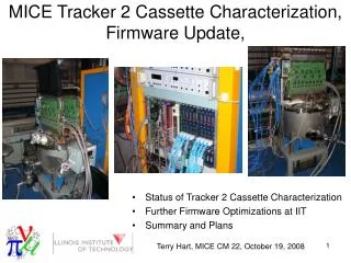
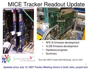
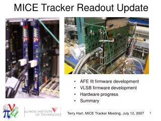
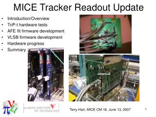
MICE Tracker Readout Update, Preparation for Cosmic Ray Tests • Introduction/Overview • AFE-IIt firmware development • VLSB firmware development • Hardware progress • Summary Terry Hart, MICE CM 19, October 7, 2007
MICE Tracker Acronyms • AFE-IIt – Analog Front End, Version II, with time • VLSB – VME LVDS Serdes Buffer • Versa Module Eurocard • Low Voltage Differential Signalling • Serializing/Deserializing • FPGA – Field Programmable Gate Array • TriP-t – Trigger with Pipeline with time • VLPC – Visible Light Photon Counter Terry Hart, MICE CM 19, October 7, 2007
Tracker Data Readout Basics Memory Bank X 4 … 1/4 of VLSB 1/4 of AFE-IIt DFPGA X 4 … AFPGA AFPGA X 4 … X 4 … ADC ADC ADC ADC Trigger and Pipeline chips - Sends bitmaps to DFPGA - Stores raw data in pipeline until receipt of MICE event trigger TriP-t TriP-t TriP-t TriP-t X 4 … Data from VLPCs
Tracker Data Readout Basics Memory Bank X 4 … 1/4 of VLSB 1/4 of AFE-IIt DFPGA X 4 … AFPGA AFPGA Analog FPGA Controls operation of TriP-t’s and ADCs. X 4 … X 4 … ADC ADC ADC ADC Trigger and Pipeline chips - Sends bitmaps to DFPGA - Stores raw data in pipeline until receipt of MICE event trigger TriP-t TriP-t TriP-t TriP-t X 4 … Event Trigger (L1ACCEPT) Data from VLPCs
Tracker Data Readout Basics Memory Bank X 4 … 1/4 of VLSB 1/4 of AFE-IIt DFPGA X 4 … AFPGA AFPGA Analog FPGA Controls operation of TriP-t’s and ADCs. X 4 … Analog to Digital Converters Digitizes raw charge and time data X 4 … ADC ADC ADC ADC Trigger and Pipeline chips - Sends bitmaps to DFPGA - Stores raw data in pipeline until receipt of MICE event trigger TriP-t TriP-t TriP-t TriP-t X 4 … Event Trigger (L1ACCEPT) Data from VLPCs
Tracker Data Readout Basics Memory Bank X 4 … 1/4 of VLSB 1/4 of AFE-IIt Digital FPGA Sets data protocol for - Bitmaps to AFPGA - Data from AFPGA DFPGA X 4 … AFPGA AFPGA Analog FPGA Controls operation of TriP-t’s and ADCs. X 4 … Analog to Digital Converters Digitizes raw charge and time data X 4 … ADC ADC ADC ADC Trigger and Pipeline chips - Sends bitmaps to DFPGA - Stores raw data in pipeline until receipt of MICE event trigger TriP-t TriP-t TriP-t TriP-t X 4 … Event Trigger (L1ACCEPT) Data from VLPCs
Tracker Data Readout Basics Formatted Data to VLSB Memory Banks Memory Bank X 4 … 1/4 of VLSB 1/4 of AFE-IIt Digital FPGA Sets data protocol for - Bitmaps to AFPGA - Data from AFPGA DFPGA X 4 … AFPGA AFPGA Analog FPGA Controls TriP-t and ADC operation. X 4 … Analog to Digital Converters Digitizes raw charge and time data X 4 … ADC ADC ADC ADC Trigger and Pipeline chips - Sends bitmaps to DFPGA - Stores raw data in pipeline until receipt of MICE event trigger TriP-t TriP-t TriP-t TriP-t X 4 … Event Trigger (L1ACCEPT) Data from VLPCs
AFE-IIt/TriP-t Basics • For MICE, average time between triggers ~ 1700 ns, but can be as short as 628 ns. (ISIS beam structure and MICE DAQ constraints) • TriP-t chips • Pipeline stores analog charge and time data. • L1ACCEPT event trigger takes time (~ 1000 ns) to be formed. • Time to digitize analog data ~ 1500 – 2000 ns. • Upon L1ACCEPT trigger, data is taken from pipeline and either • Digitized if 4-level buffer is empty or • Placed in 4-level buffer if digitization of previous event not yet done Terry Hart, MICE CM 19, October 7, 2007
AFE-IIt Firmware Modifications (AFPGA and DFPGA) Memory Bank Modifications needed for data buffering • Shorten time to digitize data • Zero suppression • End digitization series after last channel above threshold These are done. • Protocol for data transfers between DFPGA and AFPGA • Bitmaps from DFPGA to AFPGA • Digitized data from AFPGA to DFPGA This is done. • Buffer triggers in DFPGA FIFO This is nearly done. DFPGA AFPGA AFPGA ADC ADC ADC ADC TriP-t TriP-t TriP-t TriP-t Data from VLPCs
AFE-IIt Firmware Modifications (CLOCKGEN and COLLECTOR) • CLOCKGEN – clock signals for AFE-IIt boards • Input ISIS signal will vary from start to end of spill, so that AFE-IIt board will have to operate from 52.2 to 55.6 MHz. • Phase Lock Loop (PLL) to be used to lock onto variable ISIS signal 2 ms before start of spill. • Clock oscillators on AFE-IIt boards need to be replaced. • CLOCKGEN firmware has been modified to work with PLL. • Frequency locking to be tested. Terry Hart, MICE CM 19, October 7, 2007
AFE-IIt Firmware Modifications (CLOCKGEN and COLLECTOR) • COLLECTOR – sets operation modes for AFE-IIt • Variable-sized events mean that at a given time, different AFPGAs will be at different places in data acquisition-digitization-readout sequence. • Firmware modifications allow this flexibility from previous sequence which was fixed in time for all AFPGAs. • These modifications are done. Terry Hart, MICE CM 19, October 7, 2007
AFE-IIt Firmware Tests • AFE-IIt firmware package has been assembled for data readout and cosmic ray tests • AFPGA modifications (no buffering yet) • Modified D0 DFPGA (not Senerath’s) • CLOCKGEN and COLLECTOR as previously described • DFPGA output signals checked with ChipScope match code simulations • Data format • Strobe signals • Bitmaps • Digitized charges and times • AFPGA byte count Terry Hart, MICE CM 19, October 7, 2007
VLSB Firmware • VLSB = VME LVDS Serdes Buffer • Tracker data storage modules • Used for KEK test beam • Used by D0 for diagnostics • Modifications for MICE • Put event counter during spill in unused register • Put memory bank addresses of final data bytes in unused registers • Fast clear of VLSB memory • Set by bit in unused register • Fast clear done indicated another bit in unused register • Overwrite memory addresses when there’s null data so that data are stored in continuous memory blocks. • Enable Direct Memory Access block transfers VLSB memory banks storing charge and time data DFPGA directs DFPGA and AFPGA data flow AFPGA controls ADC and TriP-t operation Terry Hart, MICE CM 18, October 7, 2007
VLSB Firmware Modifications • Data storage in memory banks • Before modifications • After modifications • Newly utilized registers: used by MICE DAQ • Registers 0 – 3: Memory bank addresses of last data word • Register 15: Number of events in spill … EVENT 1 EVENT 2 EVENT 3 zeros zeros … EVENT 1 EVENT 2 EVENT 3 Terry Hart, MICE CM 19, October 7, 2007
Testing VLSB Firmware Modifications • Simulation of memory bank data, addresses, and control signals look fine. • Fast clear almost working • Simulated data written to VLSB • When fast clear bit set • Every other address (not all addresses) gets cleared • ChipScope used to investigate this. • Resolution will likely involve working out signal timing issues. • Fast clear done bit properly set after last address cleared. • Writing to other registers and squeezing out zeros will be verified soon (probably by end of week)
Preparation for Cosmic Ray Test • Finish firmware by Oct. 5 (Still working on VLSB) • Run cryostat/AFE-IIt/VLSB tracker readout tests at FNAL from Oct. 8 – 19. (Set to start) • Ship tracker readout system by Oct. 29 (was Oct. 22) • Unpack tracker readout system at RAL by Nov. 5 (may slip to Nov. 12) Terry Hart, MICE CM 19, October 7, 2007
AFE-IIt Boards • 8 boards for 2 cryostats fully tested and characterized. • 4 boards assigned to 3rd cryostat, not yet tested and characterized • 11 spare boards available, 4 of which will be assigned to 4th cryostat. • 23 AFE-IIt boards available for MICE • Malcolm has prepared document with board testing/characterization procedures for Bill, Kwame, and me. • Russ Rucinski indicated that cryostat to be ready in ~ 1 week. Terry Hart, MICE CM 19, October 7, 2007
VLSB Boards • Parts and boards are at FNAL. • Technicians have started stuffing boards. • First 1 or 2 boards may be done in ~ 1 week. • FNAL will test basic functionality of data registers. Terry Hart, MICE CM 19, October 7, 2007
Longer Term Tasks • Integrating Senerath’s DFPGA code • Senerath is working out bugs on his next-to-last and last versions • Once cosmic ray tests are set up, this will most to top of list. • Implementing and debugging AFPGA 4-level buffer • Bulk of code in place • Need to work out potential timing conflict between incoming triggers and data transfers between AFPGA/DFPGA • Testing that PLL locks on to variable ISIS signal • Hardware and firmware all set • Need to put everything together to test and work out kinks Goal: Finish these by the end of the year. Terry Hart, MICE CM 19, October 7, 2007
Summary • Preliminary firmware package being set up for data readout tests at FNAL • Only one level of 4-level buffer • Using modified D0 DFPGA instead of Senerath’s DFPGA. • Aiming for • Ship tracker readout system to RAL by Oct. 29 • Unpack tracker readout system at RAL by Nov. 5 for cosmic ray tests • Cryostat characterization and VLSB board assembly ongoing • End in sight for full firmware for MICE (~ 600 triggers/ms) Terry Hart, MICE CM 19, October 7, 2007