Download
1 / 60
600 likes | 727 Views
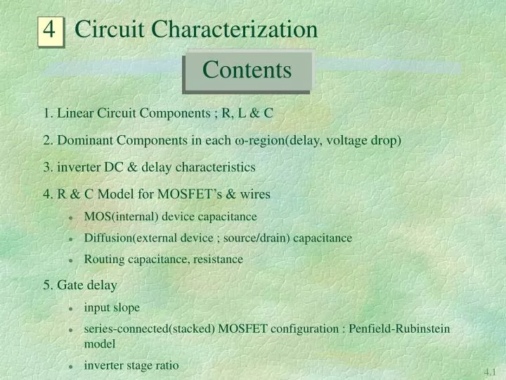
Contents. 4 Circuit Characterization. 1. Linear Circuit Components ; R, L & C 2. Dominant Components in each w -region(delay, voltage drop) 3. inverter DC & delay characteristics 4. R & C Model for MOSFET’s & wires MOS(internal) device capacitance

E N D
Contents 4 Circuit Characterization 1. Linear Circuit Components ; R, L & C 2. Dominant Components in each w-region(delay, voltage drop) 3. inverter DC & delay characteristics 4. R & C Model for MOSFET’s & wires • MOS(internal) device capacitance • Diffusion(external device ; source/drain) capacitance • Routing capacitance, resistance 5. Gate delay • input slope • series-connected(stacked) MOSFET configuration : Penfield-Rubinstein model • inverter stage ratio
6. CMOS용 inverter & Power dissipation • Static • dynamic • Short-circuit • Ring counter 7. High-Current Effects • Power/Ground bounce • EM/ESD/EOS(Electro-migration/Electro-Static Discharge/Electrical Over-Stress)
1. Linear Circuit components : R, L & C • Resistance CR) : v iR i R v i=qv V V Velocity Saturation : mean time between collision t t
Capacitance(C) : • Inductance(L) : V i v i v1 C v2 v2 V wL + v - i i
2. Dominant components V=Z • i (z = impedance) Z(w) 1) region I : C dominates 2) region II : R dominates 3) region III : L dominates wL R II III I w wc wL
3. Inverter DC & delay characteristics 1 0 0 1 load 0 seesaw rope seesaw 2 foods seesaw balance rdendez-vous seesaw • Role of inverter : 1. Signal buffering/transmission 2. Logic function
Inverter is composed of driver and load driver(transistor) characteristics Load characteristics linear triode VGS4(8V) i1 i2 VGS3(6V) VGS2(4V) VGS1(2V) VDS V12 1 out D in i2 RL i1 G 2 S
Putting them together, KCL(Kirchoff’s Current Low) demands i1=i2 VDD i RL I = (Vo-VDD) Vo i Vi Vi Vo VDD <Output Characteristics> <Transfer Characteristics> Vo Ideal RL increase Vi
Resistor, as a passive load, requires large silicon area. RL(10K) = 100 R (100 / ) Active load is better for digital purposes. VDD Large area (100 s) Vo Vi GND
: Static load line • Problems with Enhancement load 1. Slow charge/discharge due to small load current especially when Vo VDD 2. Vo cannot be raised higher than VDD-VT’ (VT’ : threshold voltage considering body effect) Vi = 5V Q1 Dynamic load line Q2 Vi = 0V VDD-VT VDD A B
i) Static Load Line : iL = iD ii) Dynamic Load Line(due to load capacitance, CL) charging(Q1 Q2) ; iD = iL - discharging(Q2 Q1) ; iD = iL + VDD iL Vo CL Vi iD Magnitude of average charging/discharging current is given as the area of AQ1Q2B
How to improve Inverter speed is how to increase charge/discharge current. • Sol. 1. Bootstrap method VDD I Vi=5V T1 X T2 Q1 Dynamic load line (due to CX) Vo CX Vi T3 Q3 Q2 Vi=0V Static load line VDD-2VT VDD VO
Sol.2 Depletion load method ID Depletion element Enhancement element ID VG=0V Depletion type VG=-1V VG=2V VTD<0 VTD>0 VG=2V VG=-2V Enhance -ment type VG=1V VG=0V VG VDD - + 0 Question) Why cannot one use depletion MOSFET as a logic element ?
Gate and Source terminals of Depletion device is tied together to suppress the Vo-dependence of iL, i.e., iL=b(0-VTD)2=b VTD 2, acting like a constant current source. VDD Vi=5V iL Vo iD iL=b(-VTD)2 Vi iD Vi=0V VDD VDS(=V0) body 효과를 고려한 부하선
VDD VDD R 0.6R VDD R D D’ R i E 0.8VDD VDD • Speed comparison between R, E, D-load VDD Eq.(1) i t = 0 Eq.(2) C Eq.(3) Charging time vs. voltage
eq(1)를 invert & integrate한 curve eq(2) t dt C = dt dV i dV E R eq(3) D’ t0 VDD VDD+VTD=0.4VD VDD-VTE=0.8VD Output voltage, V
VDD R C • 최대전류값(Vo=0일때)이 같도록 한 경우, R, E, D -부하 각각의 충전시간의 계산; R-load eq.(1)
VDD iE(v) v C E-load : -1 eq.(2) D-load : 0.4VDD<V<VDD에서는 0.6R의 저항을 통한 충전 : eq.(3)
RL RL kt SW1 t Cg Cg Cg SW2 RD Cg RD • Inverter delay() 정의) = 한 inverter가 같은 size의 연결된 inverter의 입력전압을 방전시키는 시정수 RL : depletion 소자 등가저항 RD : driver의 등가저항 ; inverter ratio = • inverter ratio k is determined as 4, from the following static consideration
t v1 v1 v2 v3 v2 4t v3 • Inverter chain에서의 충전시정수는 k=4, 방전시정수는 로 주어지며, fanout이 n이거나 부하용량이 CL=mCg인 경우, 충방전 시정수는 각각 m배!
Av: inverter 전압이득 mCgd Cs m=1-Av Cgs Cgd A B DV (1-Av)DV ; effective voltage change Av DV Total charge change input voltage change • Effective load capacitance, CL =CS+ Cgs +2 Cgd >> Cg • Miller capacitance Effective capacitance = For digital inverter (1-Av) => 2 Miller factor
4. R & C Models for MOSFET’s & wires Transistor as R
G CGS CGD D S CGB CDB CSB B MOSFET Capacitance MOSFET: 4-terminal device i) Gate capacitance off non-sat. sat.(short-channel) CGB 0 0 CGS 0 CGD 0 CG(total) 0 CG=CGS+CGD+CGB 2/3 CGS 0.5 CGD C [COX] CGB VGS lin. sat. off
ii) Junction capacitance Sidewall junction is more abrupt
iv) Routing Capacitance Csw Cf Cp: fringing cap. t Csw: sidewall cap. Cp S W Cp: planar cap. Cp Csw Assume t=const Cf W(=S) For high-(t/w), multi-bit bus, Csw dominates.
R Vj-1 R Vj R Vj+1 R C C C • Distributed RC line R = r dx (r:resistance per length) C = c dx(c:capacitance per length) : Diffusion equation (tx : time for propagating distance x)
Frequency domain solution of the distributed RC line to unit step input is as cosh(x) =
Time elapsed Distributed Lumped 0 - 90% 0 - 63% 0 - 10% RC 0.5RC 0.1RC 2.3RC RC 0.1RC • Distributed vs. Lumped R R C (Distributed) C (Lumped) Vout L D time
Characteristic of Diffusion : tx kx2 t=1 t=4 t=9 t=16 For t=410-152[ in m] I) with buffer tp = 8ns + buf ii) without buffer tp = 16ns x 0 1 2 3 4 1mm 1mm buffer
5. Gate Delay • tT = tD + ti + tslew, tslew = rslew CL • tD : internal delay of the cell ti = delay due to the intrinsic output capacitance rslew : output slew rate [ns/pF] CL : load capacitance for each output • tD = tD,O Kt Kv Kp input Ex. tQ=1.39+0.83+1.63CL tslew tD ti output KV Kt process Kp Slow typ. fast 1.34 1.00 0.72 VDD RT 3.0 3.3 3.6 -30 +90
input slope dependence (n = , : input rise time) (p = , : input fall time)
C4 A N4 C3 B N3 C2 C N2 C1 D N1 • Series-connected(stacked) MOSFET Configuration Penfield-Rubinstein model : : Summed resistance from i to power/ground : Capacitance at point i td = R1C1 + (R1+R2)C2 + (R1+R2+R3)C3 + (R1+R2+R3+R4)C4 = R1(C1+C2+C3+C4) + R2(C2+C3+C4)+R3(C3+C4)+R4C4 Elmore delay model
Elmore delay TAB = R1(C2+C3+C4 +C5 +C6 +C7 +C8 +C9 +C10) +R2( +C3+C4 +C5 +C6 +C7 +C8 +C9 +C10 ) +R3( +C4 +C5 +C6 +C7 +C8 +C9 +C10) TBD = R4( +C7 +C8 +C9) +R7( +C9) TBE = R5( +C6 +C10) +R6( +C10)
Delay Modelling i) 50%-50% delay : for multiple levels of static logic circuit
ii) 10%-90%(90-10) delay : rise time(fall time) : for precharged dynamic circuit
Delay model of interconnection driven by Rtr & terminated by CL T90% = 1.0RintCint + 2.3(RtrCint+ RtrCL+ RintCL) Rtr Rint Cint CL
Inverter Stage Ration Driving large C load using graded inverter chain fN f f2 1 Cg CL Q. Determine the scale-up factor, f minimizing total delay time for driving CL from Cg
= A. mumber of inverters, N is given by Total delay is Nf, which is to be minimized. Total delay = = * In real situation, f could be much larger than 2.7 to reduce the chip area consumption Y, i.e., N=
6. CMOS Inverter & Power Dissipation VDD S • Static Transfer Characterictic G PMOS D Vi Vo I D G NMOS S (VSS or GND) C NMOS PMOS VDD Region A cutoff linear A B D E Static power dissipation Region B sat linear Vo Region C sat sat Region D linear sat 0 VTN VDD 2 VDD Vi Region E linear cutoff VDD- VTD
Adjustment of VTN, VTP i) VTN + VTP < VDD-VSS : static current flows ii) VTN + VTP =VDD-VSS : ideal case iii) VTN +VTP >VDD-VSS : hysteresis Vi VTN PMOS NMOS VDD-VTP VTN Vi Vo VTP VDD 0 Vo Vo Both are off Vi
Influence of PN asymmetry on the transfer characteristics Vo 10 0.1 infinite transfer gain VDD Vi ideal zero output conductance
Power Consumption i) dynamic power dissipation Vi t=0 Vo Vi Vo and Substituting, (f : switching frequency) eq.(1.11)
Energy stored in CL charged up to VDD is from eq.(1.11), switching energy consumed per cycle is go ? where did
Modelling of resistive dissipation in ideal switch replace MOSFET by ideal switch in serial with a resistance, R i) In Vo’s going up ; R i Vo (indep. of R!) ; energy dissipated R in R as Vo is being raised from 0 to VDD
ii) In Vo’s going down i R R lose 1/2 store 1/2 Energy dissipated in R as CL is being discharged lose 1/2 R GND
iii) Short-circuit dissipation ref. H.J.M. Veendrick, “Short-circuit dissipation of static CMOS…” IEEE J. Solid-state Circuits, Vol. SC-19, Aug, 1984. Pp 468-473 assumption: CL = 0 Vi T r f VDD VDD-|VTP| VDD VDD/2 VTN i Vi Vo i (A) (B) imax iav t1 t2 t3 t=0
For simplicity, assume , t = tr = tf and VT = VTN = -VTP (waveform (A) = waveform(B), (A) is symmetric w.r.t t = t2 )setting