Download
1 / 16
160 likes | 395 Views
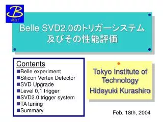
Belle SVD2.0 のトリガーシステム及びその性能評価. Contents Belle experiment Silicon Vertex Detector SVD Upgrade Level 0,1 trigger SVD2.0 trigger system TA tuning Summary. Tokyo Institute of Technology Hideyuki Kurashiro. Feb. 18th, 2004. The Belle experiment. 大量の B 中間子対 を生成して、その崩壊 時間の差から CP 対称性の破れを観測.

E N D
Belle SVD2.0のトリガーシステム及びその性能評価 • Contents • Belle experiment • Silicon Vertex Detector • SVD Upgrade • Level 0,1 trigger • SVD2.0 trigger system • TA tuning • Summary Tokyo Institute of Technology Hideyuki Kurashiro Feb. 18th, 2004
The Belle experiment 大量のB中間子対を生成して、その崩壊 時間の差からCP対称性の破れを観測 非対称パラメータ: 但し、時間差の測定は極めて困難なため 距離差を観測し、時間差に焼き直す 8GeV e- 3.5GeV e+ Dz ~ 200mm KEKB加速器@茨城県つくば市 B中間子の崩壊例
Belle Detector KL muon detector 3.5GeV e+ Super Conductive Solenoid coil 8GeV e- CsI Electromagnetic Calorimeter Time of Flight Counter Aerogel Cherenkov Counter Central Drift Chamber Silicon Vertex Detector
Silicon Vertex Detector 粒子の崩壊点を測定する検出器 両面型シリコンストリップ検出器(DSSD) をラダー状に繋げて、円筒形状に配置 Ladder 6+12+18+18 = 54 ladders 断面図(SVD2) 全体図(SVD2)
Tracking of SVD が粒子のヒット位置情報 これらをトラッキングすること で粒子の崩壊位置を決定 hadron event @ z axis rφ axis
SVD Upgrade 2003年夏、SVDをアップグレード (SVD ver.2.0) 改良点 SVD1.6 SVD2.0 acceptance 23<q<139 17<q<150 layers 3 4 radiation hardness 1Mrad >20Mrad DAQ dead time 128ms 25.6ms trigger none 128ch OR シリコンストリップ検出器としては世界初の試み!
VA1TA chip SVD2.0の読み出し回路 1Hybrid; 128 x 4chips = 512channels • VA part 128chの各ストリップからの信号を multiplexerによりシリアル化して、単一 ラインにて読み出す • TA part VAからの信号を受け取り、fastshaper によりVAよりも早く信号(トリガー)を生成 する。出力は128chの論理和(OR)で出 力される VA1TA chip(x4) Logic図
Trigger Specification VA1TAは128chの信号をシリアルに読み出す “Hold” ”readout” 2種類のトリガーが必要 シグナルを一旦ホールド その後順次読み出す • Level 0 trigger ストリップからのシグナル をホールドするためのトリ ガー (600ns以内) • Level 1 trigger ホールドした信号を取り出 すためのトリガー(2400ns) Timing diagram
SVD2.0 Trigger System Frontend Backend SVDTA(816) FADC TTM SVD_L0(36) Global _L1(1) sCDC(64) Global_L0(1) L0T TOF(32) SVD_L1(8) L1full GDL CDC-L1-rphi-full(64) L1short CDC-L1-rphi-short(64)
Trigger Logic: FADCTF FADC module 1枚でVA1TA24chip分をAD変換(Z:18枚, Rφ:18枚 ;全36枚) FADCTF SVDを18の領域(wedge)に分けて、各wedge毎にトリガーを生成 SVDTA(816ch) FADC Requirements: 3 multiplicities of 4 layers ※Left(茶)及びRight(青)の1層目 は赤を、middle(赤)の2層目は 茶と青のORを用いる SVD_L0(36bit)
Trigger Logic: Level 0 Trigger Level 0 Trigger - ストリップからの信号を ホールドするためのトリガー - SVD, sCDCのmatchingで生成 (optionでTOFを要求) - 600ns以内に生成 1μsでホールド sCDC (64bit) SVD_L0 (36bit) TOF (32bit) L0T SVD,sCDC,TOF matchingの数種類の組み合わせから、いちばんHold efficiencyの高いものを選択(1bit) SVD-sCDC-TOF matching Global_L0(1bit)
Trigger Logic: Level 1 Trigger Level 1 Trigger - ホールドした信号を取り出す ためのトリガー - SVDとCDCのmatchingで生成 - 2400nsでGDL(Global Decision Logic)に送られる SVD_L0 (36bit) CDC_L1_rphi _short (36bit) L1T L1T Information (8bit)上記例 ・matchしたtrackの本数 3 ・open event の有無 有 ・back to back event の有無 有 SVD-CDC matching SVD_L1(8bit)
< Measurement > TAに70発のテストパルスを入力して、そのカウント 数を測定 TA tuning ・Threshold の最適化 ・Hot channelのmask TAは128chOR出力 Tuning 128ch x 4chip x 2side(P/N) x 2side(Fw/Bw) x 54Ladder = 110592 channel Total: Test pulse vs count FADC threshold DSSD VA1TA Dock TTM セットアップ図 1V ~ 16500e-
Result of TA tuning (1) Threshold distribution 当初、まともなスレッショルドカーブを描くのが非常に困難であった ※N型半導体のため、N-side はノイズが大きい P-sideにも影響を及ぼす N-sideを全てdisableしてtuning(P-side:55296ch) Bad strip ~4% 2月現在 Threshold average 10500e-
Cluster energy ーVA hit ーTA hit #TA hit TA hit efficiency = #VA hit Hit efficiency Result of TA tuning (2) VA hit とTA hit の Cluster energy分布の比較 TA tuningの確認の指標 Maximum strip energy Layer毎の結果 forwardbackward L1: 0.9900.885 L2: 0.9230.910 L3: 0.9060.727 L4: 0.6260.743 Total: 83.4% 目標:88% Maximum strip energy
Summary • 2003年夏、SVDのアップグレード -アクセプタンスの増加、放射線耐性の向上、 dead timeの減少 等 -Trigger出力機能が実装された • Trigger system の構築(FADCTF, L0T, L1T) • TAのstudy ~TA tuning - threshold average 10500 e- - TA hit efficiency 83.4% • To do - hit efficiencyの更なる向上 - hot channelのmask Belle全体のtrigger systemへの導入