Download
1 / 3
30 likes | 128 Views
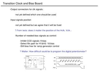
Transition Clock and Bias Board:. Output connectors for clk signals: not yet defined which one should be used Input signals position not yet defined but we agree that it will be fixed ? From tests: does it matter the position of the Hclk, Vclk... Number of needed bias signals as control:

E N D
Transition Clock and Bias Board: • Output connectors for clk signals: • not yet defined which one should be used • Input signals position • not yet defined but we agree that it will be fixed • ? From tests: does it matter the position of the Hclk, Vclk... • Number of needed bias signals as control: • Inhibit CCD signals: 9 bias • Select Mx path for H1&H3: 18 bias • Still bias free for ramp generator control • ? Walter: How difficult could be to program the digital potentiometer?
Transition Clock and Bias Board: • Ramp generator: thanks Mark! No switches AD8024 +-12v digital pot C&B board output simulation Ramp generator Output driver 400ns ~20ns step Rpot=10k. 20ns steps = 200ohms 12 volts signal ? pulse width ? from CCD test: is that fine?
Transition Clock and Bias Board: • Summary: • Connectors (input/output): • still not defined the input pinout, • output connector not decided • Ramp generator: it seems to work fine so can we go ahead with this design? • Schematics: • all devices defined in CADENCE although • connectors missing (power, output and input) • already started to put all the components together • Questions (?): interesting to know the answer • Comments: are welcome!