ENMA 490 Materials Design Fall 2002
280 likes | 301 Views
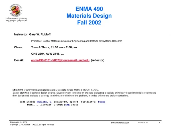
ENMA 490 Materials Design Fall 2002. Instructor: Gary W. Rubloff Professor, Dept.of Materials & Nuclear Engineering and Institute for Systems Research Class: Tues & Thurs, 11:00 am – 2:00 pm CHE 2304, AVW 2145, … E-mail: enma490-0101-fall02@coursemail.umd.edu (reflector).

ENMA 490 Materials Design Fall 2002
E N D
Presentation Transcript
ENMA 490Materials DesignFall 2002 Instructor: Gary W. Rubloff Professor, Dept.of Materials & Nuclear Engineering and Institute for Systems Research Class: Tues & Thurs, 11:00 am – 2:00 pm CHE 2304, AVW 2145, … E-mail: enma490-0101-fall02@coursemail.umd.edu (reflector) enma490.fall2002.ppt
ENMA 490Materials DesignFall 2002 DESCRIPTION This is the senior capstone design course for materials science and engineering. Design is a key theme in materials science and engineering, delivering solutions from the understanding achieved by analysis. Design also opens the door to creativity and invention. New materials are revolutionizing many areas of advanced technology. This is a design project course in which the students will work as a team. They will survey some of the exciting areas of new materials and microsystems, and they will identify opportunities where the inclusion of new materials can markedly advance microsystem design. The goal is to develop a design for a microdevice, including materials choice and process sequence, which capitalizes on the properties of new materials. enma490.fall2002.ppt
ENMA 490Materials DesignFall 2002 MECHANICS Class periods are designated as 2X/week, 3 hrs each. We will use them as it makes sense to the class. REQUIREMENTS Ongoing presentations and discussions in class Final report Final presentation GRADES Distribution determined by individual contributions to progress and to team-building Center of distribution determined by accomplishment and effort of entire team enma490.fall2002.ppt
StudentsENMA 490 fall 2002 enma490.fall2002.ppt
AJC Online (Blackboard site) www.ajconline.umd.edu Use your regular userid and password from GLUE or WAM to login enma490.fall2002.ppt
Your Personal Blackboard Site enma490.fall2002.ppt
ENMA 490 Blackboard Site enma490.fall2002.ppt
New Materials enma490.fall2002.ppt
Al => Cu metallurgy SiO2 => low K insulators submicron vertical profiles Al 3.0 u-cm Cu 1.7 u-cm SiO2, K=4.0 Low K K=2.0 40 & Strip 35 & Strip • high aspect ratio • Interconnects • (height/width) device with Al & SiO2 interconnects 30 25 plasma processing => directional etching device with Cu & low K interconnects Delay in ps 20 15 G. S. Oehrlein 10 device alone 5 chemical vapor deposition => metal filling 0 0.65 0.5 0.35 0.25 0.18 0.13 0.1 Generation (MFS, µm) G. W. Rubloff J. N. Kidder, Jr. Data From: Bohr, Mark T; “Interconnect Scaling -The Real Limiter to High Performance ULSI”; Proceedings of the 1995, IEEE International Electron Devices Meeting; pp241-242 KA Monnig, Sematech 09/02/96 Interconnects ControlCircuit Performance enma490.fall2002.ppt
liquid source chemical vapor deposition AlCuSi interconnect W stud gate insulator G D S DRAM capacitor • Device applications SrBi2Ta2O9 ultrathin gate dielectrics for FET’s and DRAM’s ferroelectric nonvolatile memory cell cross-section Complex New Materials • Insulators High dielectric constants Replace/complement traditional SiO2 & Si3N4 J. N. Kidder, Jr. R. Ramesh NSF MRSEC enma490.fall2002.ppt
Ferroelectrics : Crystal Structure R. Ramesh enma490.fall2002.ppt
Spontaneous Polarization Lead Zirconate Titanate Strontium Bismuth Tantalate Large Dielectric Constants Barium Strontium Titanate Pyroelectric Effects Lead Titanate Lead Scandium Tantalate Electro-Optic Effects Potassium Tantalate Niobate Lead (La) Zirconate Titanate Microwave Properties Barium Strontium Titanate World of Ferroelectrics O. Auciello, J.F. Scott, R. Ramesh Volume 51 #7, 22 (1998) R. Ramesh enma490.fall2002.ppt
Device Applications of Ferroelectric Thin Films R. Ramesh enma490.fall2002.ppt
COS : Metallic Perovskite Templates: LSTO on Si Metal LSCO CMP Glass SrTiO3 PZT LSCO LSTO or LSTO/NbSTO or SRO Epi-Si Plug 100 nm Drain Metal 1 LSCO 2 nm PZT LSCO LSTO Si Si Ramesh / Schlom, (UMCP / PSU) APL, in press (2002) enma490.fall2002.ppt
New Processes for Making New Materials enma490.fall2002.ppt
ALD Process Cycle enma490.fall2002.ppt
Materials Capabilityfrom ALD Process enma490.fall2002.ppt
Hafnium Silicate ALD • Motivation: high-K dielectric to replace SiO2 as FET gate dielectric R. Gordon, ALD 2001 enma490.fall2002.ppt
ALD Precursor Potential R. Gordon, ALD 2001 enma490.fall2002.ppt
Microdevices for Microsystems (MEMS) enma490.fall2002.ppt
Shut-Off Valve Normally open, proportional Normally closed, positive shut-off http://www.redwoodmicro.com/presentations/SEMICON2001_files/frame.htm enma490.fall2002.ppt
Micro-Engine • Portable power source with 10X power density of state-of-art batteries • MIT microturbine project R. Ghodssi et. al. (UMCP) enma490.fall2002.ppt
Optical MEMS (MOEMS) Programmable micromirrors Texas Instruments digital light processing (InFocus PC projector) NASA programmable optics for next-generation telescope Optical communications Information transfer via optical signals Fiber optics or wireless (free-space) Optoelectronics Computing with light 750K DMD’s in TI device http://www.dlp.com/dlp/home.asp NASA (C. Stahle) Low-stress Si3N4 shutters and hinges Pop-up detectors Sandia pop-up mirror and drive system http://mems.sandia.gov/scripts/images.asp enma490.fall2002.ppt
Chemical Sensors Thin film materials as chemical sensors Electrical, mechanical, or other properties respond to chemistry and are measured as readout NIST-UMD microhotplate-based artificial nose Thin film SnO adsorbs chemical species Resistance change measured electrically Sensor thin film fabricated on microhotplate for rapid temperature cycling Signal processing algorithms and programmed temperature-time cycles to achieve selectivity, sensitivity, and coverage for multiple chemical species Challenges Chemical response Materials Device reliability http://www.enme.umd.edu/SSSC/ enma490.fall2002.ppt
Advanced Materials Applied to MEMS enma490.fall2002.ppt
Varying patterns Smart Materials for MEMS Shape memory alloys (SMA) to exploit novel mechanical properties of SMA films Patterned, graded, and blanket films Patterned NiTi films on Si cantilever substrate M. Wuttig enma490.fall2002.ppt
ENMA 490 Materials DesignFall 2002 DESCRIPTION This is the senior capstone design course for materials science and engineering. Design is a key theme in materials science and engineering, delivering solutions from the understanding achieved by analysis. Design also opens the door to creativity and invention. New materials are revolutionizing many areas of advanced technology. This is a design project course in which the students will work as a team. They will survey some of the exciting areas of new materials and microsystems, and they will identify opportunities where the inclusion of new materials can markedly advance microsystem design. The goal is to develop a design for a microdevice, including materials choice and process sequence, which capitalizes on the properties of new materials. OPERATIONS Students have the primary responsibility to investigate new materials and microsystems, identify opportunities, and develop designs to realize those opportunities. The class team should plan its activities and timelines, coordinate its progress, and periodically present reports in class. enma490.fall2002.ppt
What’s Next? • Organize mechanics for collaboration? • Identify information sources? • Brainstorm answers? • Develop initial scope of new materials? • Develop picture of MEMS devices and applications? • Outline a ficticious answer to see what’s involved? • Develop bibiography? • Review past materials course notes and textbooks? • Talk to faculty working in these areas? • Create a project timeline? • Start a list of invited speakers? • …. enma490.fall2002.ppt
