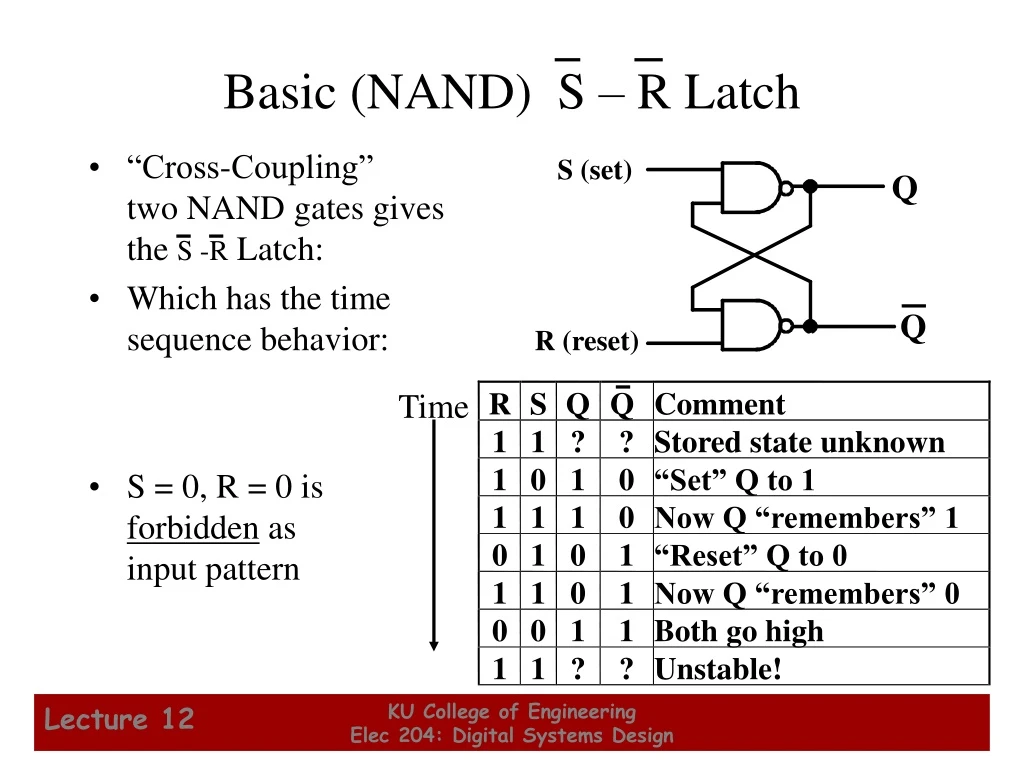
Basic (NAND) S – R Latch
250 likes | 305 Views
Learn about S-R latch, clocked S-R latch, D latch, flip-flops, and the latch timing problem in digital systems design. Explore different solutions and behaviors.

Basic (NAND) S – R Latch
E N D
Presentation Transcript
Q R S Q Q Comment 1 1 ? ? Stored state unknown 1 0 1 0 “Set” Q to 1 1 1 1 0 Now Q “remembers” 1 0 1 0 1 “Reset” Q to 0 Basic (NAND) S – R Latch S (set) Q • “Cross-Coupling” two NAND gates gives the S -R Latch: • Which has the time sequence behavior: • S = 0, R = 0 is forbidden as input pattern R (reset) Time 1 1 0 1 Now Q “remembers” 0 0 0 1 1 Both go high 1 1 ? ? Unstable! KU College of Engineering Elec 204: Digital Systems Design
R (reset) Q Q S (set) Time R S Q Q Comment 0 0 ? ? Stored state unknown 0 1 1 0 “Set” Q to 1 0 0 1 0 Now Q “remembers” 1 1 0 0 1 “Reset” Q to 0 0 0 0 1 Now Q “remembers” 0 1 1 0 0 Both go low 0 0 ? ? Unstable! Basic (NOR) S –R Latch • Cross-coupling twoNOR gates gives theS – R Latch: • Which has the time sequence behavior: KU College of Engineering Elec 204: Digital Systems Design
S Q C Q R Clocked S - R Latch • Adding two NANDgates to the basicS - R NAND latchgives the clockedS – R latch: • Has a time sequence behavior similar to the basic S-R latch except that the S and R inputs are only observed when the line C is high. • C means “control” or “clock”. KU College of Engineering Elec 204: Digital Systems Design
S Q C Q R Clocked S - R Latch (continued) • The Clocked S-R Latch can be described by a table: • The table describeswhat happens after theclock [at time (t+1)]based on: • current inputs (S,R) and • current state Q(t). KU College of Engineering Elec 204: Digital Systems Design
D Q C Q Q D Q(t+1) Comment 0 0 0 No change D Q 0 1 1 Set Q 1 0 0 Clear Q Q C 1 1 1 No Change D Latch • Adding an inverterto the S-R Latch,gives the D Latch: • Note that there areno “indeterminate”states! KU College of Engineering Elec 204: Digital Systems Design
Flip-Flops • The latch timing problem • Master-slave flip-flop • Edge-triggered flip-flop • Standard symbols for storage elements • Direct inputs to flip-flops • Flip-flop timing KU College of Engineering Elec 204: Digital Systems Design
The Latch Timing Problem • In a sequential circuit, paths may exist through combinational logic: • From one storage element to another • From a storage element back to the same storage element • The combinational logic between a latch output and a latch input may be as simple as an interconnect • For a clocked D-latch, the output Q depends on the input D whenever the clock input C has value 1 KU College of Engineering Elec 204: Digital Systems Design
Y Clock Clock D Q Y Q C The Latch Timing Problem (continued) • Consider the following circuit: • Suppose that initially Y = 0. • As long as C = 1, the value of Y continues to change! • The changes are based on the delay present on the loop through the connection from Y back to Y. • This behavior is clearly unacceptable. • Desired behavior: Y changes only once per clock pulse KU College of Engineering Elec 204: Digital Systems Design
The Latch Timing Problem (continued) • A solution to the latch timing problem is to break the closed path from Y to Y within the storage element • The commonly-used, path-breaking solutions replace the clocked D-latch with: • a master-slave flip-flop • an edge-triggered flip-flop KU College of Engineering Elec 204: Digital Systems Design
S S S Q Q Q C C C R R Q R Q Q S-R Master-Slave Flip-Flop • Consists of two clockedS-R latches in serieswith the clock on the second latch inverted • The input is observedby the first latch with C = 1 • The output is changed by the second latch with C = 0 • The path from input to output is broken by the difference in clocking values (C = 1 and C = 0). • The behavior demonstrated by the example with D driven by Y given previously is prevented since the clock must change from 1 to 0 before a change in Y based on D can occur. KU College of Engineering Elec 204: Digital Systems Design
Master-Slave FF Operation KU College of Engineering Elec 204: Digital Systems Design
Master-Slave FF Operation KU College of Engineering Elec 204: Digital Systems Design
Master-Slave FF Operation KU College of Engineering Elec 204: Digital Systems Design
Flip-Flop Problem • The change in the flip-flop output is delayed by the pulse width which makes the circuit slower or • S and/or R are permitted to change while C = 1 • Suppose Q = 0 and S goes to 1 and then back to 0 with R remaining at 0 • The master latch sets to 1 • A 1 is transferred to the slave • Suppose Q = 0 and S goes to 1 and back to 0 and R goes to 1 and back to 0 • The master latch sets and then resets • A 0 is transferred to the slave • This behavior is called 1s catching KU College of Engineering Elec 204: Digital Systems Design
Flip-Flop Solution • Use edge-triggering instead of master-slave • An edge-triggered flip-flop ignores the pulse while it is at a constant level and triggers only during a transition of the clock signal • Edge-triggered flip-flops can be built directly at the electronic circuit level, or • A master-slave D flip-flop which also exhibits edge-triggered behavior can be used. KU College of Engineering Elec 204: Digital Systems Design
D D S Q Q Q C C C Q R Q Q Edge-Triggered D Flip-Flop • The edge-triggered D flip-flop is thesame as the master-slave D flip-flop • It can be formed by: • Replacing the first clocked S-R latch with a clocked D latch or • Adding a D input and inverter to a master-slave S-R flip-flop • The delay of the S-R master-slave flip-flop can be avoided since the 1s-catching behavior is not present with D replacing S and R inputs • The change of the D flip-flop output is associated with the negative edge at the end of the pulse • It is called a negative-edge triggered flip-flop KU College of Engineering Elec 204: Digital Systems Design
D D S Q Q Q C C C Q R Q Q Positive-Edge Triggered D Flip-Flop • Formed byadding inverterto clock input • Q changes to the value on D applied at the positive clock edge within timing constraints to be specified • Our choice as the standard flip-flop for most sequential circuits KU College of Engineering Elec 204: Digital Systems Design
Edge-Triggered FF Operation KU College of Engineering Elec 204: Digital Systems Design
Edge-Triggered FF Operation KU College of Engineering Elec 204: Digital Systems Design
Edge-Triggered FF Operation KU College of Engineering Elec 204: Digital Systems Design
Edge-Triggered FF Operation KU College of Engineering Elec 204: Digital Systems Design
S S D D R R C C D with 0 Control SR D with 1 Control SR (a) Latches S S D D C C R R C C Triggered D Triggered D Triggered SR Triggered SR (b) Master-Slave Flip-Flops D D C C Triggered D Triggered D (c) Edge-Triggered Flip-Flops Standard Symbols for Storage Elements • Master-Slave:Postponed outputindicators • Edge-Triggered:Dynamicindicator KU College of Engineering Elec 204: Digital Systems Design
S D Q C Q R Direct Inputs • At power up or at reset, all or partof a sequential circuit usually isinitialized to a known state beforeit begins operation • This initialization is often doneoutside of the clocked behaviorof the circuit, i.e., asynchronously. • Direct R and/or S inputs that control the state of the latches within the flip-flops are used for this initialization. • For the example flip-flop shown • 0 applied to R resets the flip-flop to the 0 state • 0 applied to S sets the flip-flop to the 1 state KU College of Engineering Elec 204: Digital Systems Design
Flip-Flop Timing Parameters t t $ wH wH,min t t $ C wL wL,min t t s h / R S • ts - setup time • th - hold time • tw - clockpulse width • tpx - propagation delay • tPHL - High-to-Low • tPLH - Low-to-High • tpd - max (tPHL, tPLH) t p-,min t p-,max Q (a) Pulse-triggered (positive pulse) t t $ wH,min wH t t $ C wL wL,min t t s h D t p-,min t p-,max Q (b) Edge-triggered (negative edge) KU College of Engineering Elec 204: Digital Systems Design
Flip-Flop Timing Parameters (continued) • ts - setup time • Master-slave - Equal to the width of the triggering pulse • Edge-triggered - Equal to a time interval that is generally much less than the width of the the triggering pulse • th – minimum hold time for the inputs - Often equal to zero • tpx - propagation delay • Same parameters as for gates except • Measured from clock edge that triggers the output change to the output change KU College of Engineering Elec 204: Digital Systems Design