Download
1 / 51
510 likes | 786 Views
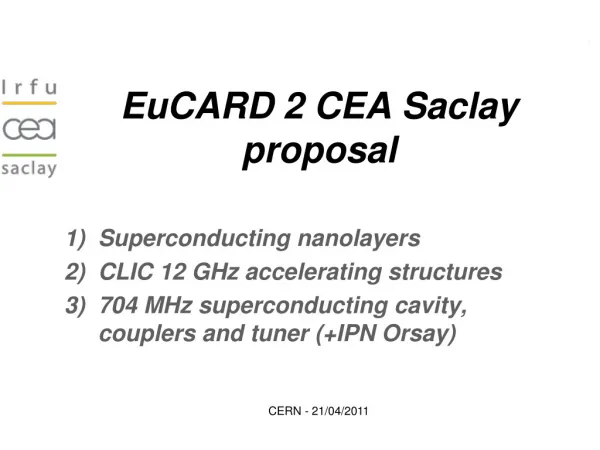
EuCARD 2 CEA Saclay proposal. Superconducting nanolayers CLIC 12 GHz accelerating structures 704 MHz superconducting cavity , couplers and tuner (+IPN Orsay). CERN - 21/04/2011. 1) Superconducting Nano-layers : a new family of materials specially adapted to SRF performances.

E N D
EuCARD 2 CEA Saclay proposal Superconductingnanolayers CLIC 12 GHz accelerating structures 704 MHz superconductingcavity, couplers and tuner (+IPN Orsay) CERN - 21/04/2011
1)Superconducting Nano-layers : a new family of materials specially adapted to SRF performances
Limits in a RF cavity 1.5 GHz Nb3Sn cavity (Wuppertal, 1985) 1.3 GHz Nb cavity (Saclay, 1999) Classical theory BCS + RF : • Magnetic RF field limits Eacc:Eacc HRF • Phase transition when magnetic HRF ~> HSH (superheating field) • For Nb HSH ~1,2.HC(thermodynamic) • Higher Tc => higher Hc => higher Eacc But… • Bulk Nb3Sn cavity : relative failure • High Q0 @ low field => low surface resistance => good quality material • Early Q slope !!! • Note : • BCS valid only near TC , clean limit • we work at 2 K + rather dirty limit. • BCS model needs to be completed Nb3Sn (Hc = 0.54 T) Nb (Hc = 0.2 T)
High field dissipations : due to vortices ? 1.5 GHz Nb3Sn cavity (Wuppertal, 1985) 1.3 GHz Nb cavity (Saclay, 1999) Theoretical Work from Gurevich : temperature correction • Non linear BCS resistance at high field : quadratic variation of RBCS • Vortices : normal area ~ some nm can cause “hot spots” ~ 1 cm (comparable to what is observed on cavities) • At high field vortices => thermal dissipation @ vortices => Quench • Nb is the best for SRF because it has the highest HC1, (prevents vortex penetration) Nb3Sn (Hc1 = 0.05 T) • Nb is close to its ultimate limits (normal state transition) • avoiding vortex penetration => keep below HC1 • increasing the field => increase HC1 • “invent” new superconductors with HC1> HC1Nb Nb (Hc1 = 0.17 T) A. Gurevich, "Multiscale mechanisms of SRF breakdown". Physica C, 2006. 441(1-2): p. 38-43 A. Gurevich, "Enhancement of RF breakdown field of SC by multilayer coating". Appl. Phys.Lett., 2006. 88: p. 12511. P. Bauer, et al., "Evidence for non-linear BCS resistance in SRF cavities ". Physica C, 2006. 441: p. 51–56
Breaking Niobium monopoly x 200 • Overcoming niobium limits (A.Gurevich, 2006) : • Keep niobium but shield its surface from RF field to prevent vortex penetration • Usenanometric films (w. d < l) of higher Tc SC : => HC1enhancement • Example : • NbN , x = 5 nm, l = 200 nm • => HC1 = 0,02 T • 20 nmfilm => H’C1 = 4,2 T (similar improvement with MgB2 or Nb3Sn) Bulk Happlied • high HC1 => no transition, no vortex in the layer • applied field is damped by each layer • insulating layer prevents Josephson coupling between layers • applied field, i.e. accelerating field can be increased without high field dissipation • thin film w. high Tc => low RBCS at low field => higher Q0 HNb Cavity's internal surface → Outside wall
High Tc nanometric SC films : low RS, high HC1 • In summary : take a Nb cavity… • deposit composite nanometric SC (multilayers) insideNb / insulator/ superconductor / insulator /superconductor… Magnetic field B (mT) Quality coefficient Q0 Accelerating Field Eacc (MV/m) INCREASE Eacc AND Q0 !!!
First exp. results on highquality model samples ~ 12 nm NbN x 4 14 nm insulator (MgO) 250 nm Nb “bulk” Monocrystalline sapphire Test sample ML • Choice of NbN: • ML structure = close to Josephson junction preparation (SC/insulator compatibility) • Use of asserted techniques for superconducting electronics circuits preparation: • Magnetron sputtering • Flat monocrystalline substrates ~ 25 nm NbN ~ 15 nm insulator (MgO) Reference sample R 250 nm Nb “bulk” Test sample SL Monocrystalline sapphire • Collaboration with J.C. Villégier, CEA-Inac / Grenoble
Local magnetometry (1) Differential Locking Amplifier Excitation/Detection coil (small/sample) = T/Tc • 3rd harmonic measurement, collaboration INFM Napoli • local measurement : sample size >> excitation/measuring coil • perpendicular field @ Napoli (// field underdevelopment @ Saclay) • b0cos (wt) applied in the coil • temperature ramp • third harmonic signal appears @ BC1 increasing I = increasing B TCi at Bi Sample SL : third harmonic signal for various b0
Local magnetometry (2) Nb « bulk » / MgO Nb « bulk » / MgO/ NbN 25 nm • SL sample : 250 nm Nb + 14 nm MgO + 25 nm NbN • 8.90K < Tp° < 16K : behavior ~ NbN alone • Tp°< 8.90K, i.e. when Nb substrate is SC , => BC1SL >> BC1Nb
Local magnetometry + SQUID measurement @ 4,5K 2k, 200 mT local magnetometer under development @ Saclay • SL sample : 250 nm Nb + 14 nm MgO + 25 nm NbN • Tp°< 8.90K, i.e. when Nb substrate is SC , => BC1SL >> BC1Nb • Need to extend measure @ higher field and lower temperature
What is needed (1)? Phase 1: Model samples (1 y.) / Phase 2 : Realistic samples (1y.)/ Phase 3 Demonstration @ 1,3 GHz (2Y) Thin film deposition : other collaborations in negotiation : CERN CGE (Fr) Jlab(USA)… Coordination IRFU Phase 1 Modeling, theoretical approach, structure specification IRFU 1 post doc Nb Model samples deposition + characterization INAC 1 post doc MgB2 Model samples deposition + characterization INFM + subcontractors (? 1 PhD student + 50 k€) Magnetic measurement IRFU optimization of deposition ALD: INPG deposition set-up ~ 100k€ Results analysis Phase 2
What is needed (2)? Phase 1: Model sample (1 y.) / Phase 2 : Realistic samples (1y.) / Phase 3 Demonstration @ 1,3 GHz Sample deposition: Sputtering ALD Hollocathode HIPIMS…. ML on mono- crystalline saphire ML on mono- And poly- crystalline niobium Complex structures on copper TE011, ~3 GHz IPNO Magnetic measurement IRFU Sample cavities tests IPNO/LKB Results analysis Selection of deposition technique “sample” cavities Existing set-ups : small improvement investments (< 50k€) Phase 3 50 GHz LKB
What is needed (3)? Phase 1: Model sample (1 y.) / Phase 2 : Realistic samples (1y.) / Phase 3 Demonstration @ 1,3 GHz • Design must be chosen after comparison of performances on samples deposited with various deposition techniques • Measurement on 1,3 GHz will achieve a demonstration of feasibility cavity set up design cavity set up construction Sub contract Typically 100 k€ Cavity deposition IRFU RF measurement IRFU 1.3 GHz Irfu DEMONSTRATION !
Summary • 4 years program • 3 labs in the task and possibly up to 5 labs
Conclusions & perspectives: • If theoretical approach from Gurevich gets confirmed MULTILAYERS = only way to go beyond Nb !!!! • Main challenge : thin film deposition inside cavities • They are recent promising developments in deposition techniques (ALD, HIPIMS…) => collabn with materials labs. • Multilayers can be deposited inside existing cavities => upgrade of existing facilities • Improvement expected for EaccAND Q0 : all SRF application can benefit from this technology !
2) CLIC X-band accelerating structure R&D F. Peauger 21th April 2011
Context of the X-band activitiesat CEA Saclay • CEA entered in the CLIC collaboration with the construction of the Probe Beam Linac CALIFES in CTF3 (in 2005) • Exceptional contribution of France to CERN • CTF3 contributions: • HV modulator and RF components for the CERN klystron test stand and TBL line • Accelerating structures for the Two Beam Test Stand • Period : 2008 – 2012, Budget = 1 M€ - 48 persons-months (p.m.) Accelerating structures (fabrication in progress) HV Modulator RF Components
Wakefield monitor development for CLIC accelerating structures GdfidL simulation of TM modes, beam offset dx = 1 mm • Wakefield Monitors = Beam Position Monitors integrated to the accelerating structures • Allows beam-based alignment of structures to remove wakefield effects and emittance growth • Emittance growth very well improved by aligning the structure to an accuracy of 5 µm 18 GHz DX DY • Accelerating Structure features : • TD24 (CERN design) without RF absorbers • 100 MV/m accelerating gradient • 24 tapered cells with 2/3 phase advance at 12 GHz with mean aperture of 5.5 mm • dipole mode above 16 GHz • WFM features : • WFM = Two coaxial rf pick-ups on the middle cell damping wg • on large side wg for TM-like modes • on small side wg TE-like modes Hybrid HEM modes in the cell generated by an offset beam
Integration in the Two Beam Test Stand in CTF3 Vacuum RF feedthroughs on CF flange Accelerating Structure n°1 Accelerating Structure n°2 Beam Trajectory Input RF power Vacuum tank not shown Installation in 2011
RAW MATERIAL OFE COPPER Fabrication process of X band structures ACCELERATING STRUCTURE READY FOR TEST - CLIC baseline- Fabrication of three structures in progress in collaboration with CERN
Industrial partner for ultra-precision machining • Tolerance = 2.5 µm • Surface roughness = 25 nm • Flatness = 2 µm • Large investment of our supplier : • Machining equipment: • 1 nm programming resolution • hydrostatic oil bearing slides • linear motors • thermal stabilization at +/- 0.05°C • Interferometers for roughness and flatness control without contact • Cutting tools: • Monocristal diamond for milling and turning Surface roughness of 1.5 nm achieved
Why an R&D on X band structures ? • X band technology becomes more and more attractive : • CLIC main linac frequency • Growing interest for FEL and compact light sources (PSI, ELETTRA, Univ. Groningen, SLAC, LANL, LLNL…) • But : • Few statistic results ,100 MV/m demonstrated on few structures only, • Surface damages still present, even with good breakdown rate • Some breakdown theories exists, but no clear experimental demonstration • Very difficult to fabricate • Tight tolerances • Few industrial capabilities: fabrication costs and delays are high • Full feature not tested yet (HOM absorbers, wakemonitors, etc…)
EuCARD 2 proposal • Design, fabrication and test of “12 GHz prototype structures “ • As close as possible to the CLIC requirements • 100 MV/m, TW with low vg, HOM damping with RF absorbers • compact couplers, WFM, vacuum tightness and cooling circuits • (80-90 % alreadydesigned by CERN) • Short structures could help for the statistic demontration (reduced nbof cells) • Alternative material configurations, fabrication process and preparation techniques • Use of large grain copper to reduce atomic diffusion and breakdown probability (or mixed grain sized ?) • Bead pull measurement test bench at CEA Saclay • Fundamental mode tuning and HEM modes measurement for wakefield monitors • “Mid power” test bench at CEA Saclay • ~ tens of kW peak power with TWT and pulse compressor • Multipactorstudy in rfabsorbers and WFM • Preparation of the structures for high power tests (pre-processing?) CERN design example
The 12 GHz Power station project at CEA Saclay • Independant operation to CTF3 • Proximity with chemical lab and clean room Specifications : RF Frequency: 12 GHz Peak power: 120 MW Pulse length: 300 ns Repetition rate: 50 Hz • Main features: • Modulator HT 430 kV • Klystron 50 MW – 1.5 µs • RF Pulse compressor SLED • LLRF withfast phase modulation Klystron Test structure area RF Pulse compressor Modulator Ressources of thisproject not asked in Eucard 2 24
Budget, schedule and collaborations • Rough schedule: • Year 1-2 : Design and manufacture of the structures, test bench study and construction • Year 3-4 : High power tests of the structures • Possible collaborations: • CERN for structure design, fabrication and high power testing • PSI for high power testing ? • Cockcroft Institute ? Cost estimation: * not includehigh power tests costs
3) Development of critical components for high power accelerators CEA Saclay proposals for 704 MHz cavity and couplers G. Devanz – S. Chel 21th April 2011
Introduction Several laboratories are involved in programs aiming at designing and prototyping sc cavities and components for high intensity proton linacs (SPL, ESS, MYRRHA, …) R&D programmes already supported such developments, in particular in the frame of CARE (FP6) and EuCARD (FP7). Progress done on several critical components makes them available for European Research Infrastructures which are now in construction. We propose to proceed with the same spirit in order to increase the performances of some components and to make them fit with future linac design and/or parameters.
High beta cavity development in EuCARD Achievements in FP7-EuCARD: Optimized RF and mechanical design of a 704 MHz b=1 elliptical sc cavity Fabrication and test in Vertical cryostat of cavity 704 MHz • assymetriccavity • beam tube ø140 mm with a ø100 mm port for power coupler • beam tube ø130 mm with a ø10 mm port for pick-up probe • stiffening rings between adjacent cells • eachbeam tube equippedwith one ø40 mm HOM port
Helium tanks for 704 MHz b=1 cavities The prototype fits on our frames for surface preparation (BCP, VEP, HPR) and test in vertical cryostat In order to be able to perform qualification tests in horizontal cryostat CryHoLab, this prototype can be equipped with tuner, coupler, He tank, … CryHoLab • power coupler port cooled by LHe • interfaces for lateralfrequency tuner ready (similar to Saclay IV) • Helium tank made of Ti
High beta cavity characterization • First proposal for EuCARD2 : completion of RF tests in CryHoLab • Several components will be ready in 2013 (tuner, support, He tank) • Cryo and RF test stand already qualified • Magnetic shielding still to be studied and fabricated • Qualification of the Helium tank design ; cryogenic behavior ; freq. tuner and LFD
SPL and ESS requirements With our set of cavity and beam parameters: SPL:Qex,opt= 1.2 e6 and Pbeam= Pin,max= 1.03 MW ESS:Qex,opt= 6 e5 and Pbeam= Pin,max= 0.8 to 1.2 MW • → Typical RF power in the MW range • From recommandations of RF experts, following tests are required: • 2 MW peak power with a limited pulse length • nominal peak power with the nominal average power
Power couplers for 704 MHz sc cavities Coupler developments: In the previous FP6/HIPPI program, we started the development of a high power coupler operating in pulsed mode G. Devanz designed most of the critical parts (doorknob, window, LHe and water cooling circuits, …) for 1 MW at 10% duty cycle required for operation of high intensity proton linacs 100 mm diameter 50 W impedance doorknob (air) vacuum gauge He cooledouterconductor electropolished water cooled innerconductor water cooled RF window cryostat flange
704 MHz coupler test stand at RT Coupler assembly in Clean Room Coupler processing in horizontal position Two couplers successfully processed at RT up to 1.2 MW peak @10% DC in TW for 300hrs
Qualification of 700 MHz – 1 MW coupler at cold • Assembly of one coupler on HIPPI cavity (700 MHz, b=0.5) in ISO4 CR, and installation in test cryostat CryHoLab • Only short time of RF processing in full reflectionwasnecessary to reachhigh power levels • Cavity (off resonance) and coupler operationat 1MW full duty cycle for severalhours • Efficient counter-flow GHecooling of the coupler leading to limitedheattransfer to the LHe bath Qualification of 704 MHz power coupler on sc cavity at 2 K operated at Ppeak= 1.1 MW with tpulse= 2 ms and freq = 50Hz
2-ports SC cavity for coupler qualification in TW RFout • In the previous test: coupler tested with a “off resonance” cavity (open circuit) • Coupler tested in a standing wave regime: • Spatially fixed field extrema • Not easy to sweep along the coax • In order to test the coupler in a beam configuration, i.e. all the RF is absorbed by the beam and the coupler is working on a travelling wave regime (TW), we use a 2-port cavity • This superconductive cavity would allow tests at 2 K in CryHoLab RFin TW regime for the coupler = beam configuration
RF vacuum gaskets for couplers RF Al-Mg « diamond » gasket Conflatwith RF contact RF Flanges • Severalcombinations of flangematerials possible (NbTi+NbTi, NbTi+SS, …) • RF boundary not optimized (exposedflangematerial) • good RF and geometricalcontinuity • Large diameters ~100 mm: onlystainlesssteelflanges New Al-Mg « RF » gasket Optimization of Al-Mg gasket for RF New gasket profiles Need prototypes and tests
Qualification of 700 MHz – 1 MW coupler at 4 K 704 MHz – MW(s) coupler • Second proposal for EuCARD2 : • a) power tests of 704 MHz couplers in full TW mode at 1 MW • optimization of some coupler parts (DoorKnob, RF gaskets, ???) • fabrication of a pair of couplers • design and fabrication of a 2-ports cavity • qualification tests in CryHolab • b) power tests of 704 MHz couplers in full TW mode at 2 MW 704 MHz Power Station 2-ports SC cavity Vacuum RF flange Upgrade at 2 MW foreseen
Power test stand: 2 MW upgrade The SUPRAtech platform at Saclay is equipped with a 704 MHz power station with a single klystron delivering a maximum of 1 MW maximum peak power and 100 kW average. An upgrade is foreseen up to 2 MW using a second klystron + RF combiner (2013 – 2014) 2 MW upgrade Ressources of thisupgrade not asked in Eucard 2
Development of critical components for high power accelerators IPN-Orsay proposal for 352 MHz freq tuner
New tuning system for Spoke cavity • GOAL: study, fabrication and test at cold temperature of an innovative tuning system for multi-gaps Spoke cavity in pulsed regime. 352 MHz, beta 0.30, Triple Spoke « Classical » tuning system by deformation
New tuning system for Spoke cavity • PROBLEMS: • In pulsedoperation need to increasecavitystiffness to compensate for the Lorentz forces detuning • Applied forces on the cavitybecomerelativelyhigh • Tuning system becomesbulky and shows thermal gradients • IDEA: Develop a tuning system WITHOUT deforming the cavity body use of a superconducting plunger EM simulations on Triple-Spokecavity Preliminarystudy of a plunger for Spokecavity
IPN Orsay proposal for Spoke cavity tuner RF Coupler RF amplifier Plunger + Triple-Spokecavity Third proposal for EuCARD2 : Design and fabrication of a new frequency tuner Study of LFD compensation with tests at cold with existing RF coupler
Local magnetometry (4) • Sample SL : small Nb signal @ ~TcNb : Nb is sensed through the NbN layer ! • Since the Nb layer feels a field attenuated by the NbN layer, the apparent transition field is higher. • This curve provides a direct measurement of the attenuation of the field due to the NbN layer BC1 curves for Niobium in the reference (direct measurement) and in SL (under the NbN layer).
Adjustment of coil distance glue glue + copperpowder glass bead wedge : 60 µm coil
Multilayers optimization Nb NbN Al2O3 MgO Cu Metallic substrates more realistic): • SC structure optimization • Deposition techniques optimization • Magnetron sputtering Inac (Grenoble), • Atomic Layer Deposition INP (Grenoble) • From samples to cavities : • ALD involves the use of a pair of reagents • Application of this AB Scheme • Reforms a new surface • Adds precisely 1 monolayer • Viscous flow (~1 Torr) allows rapid growth • No line of site requirements • => uniform layers, larges surfaces, well adapted to complex shapes : cavities! • up grade of existing cavities ?
Bulk Nb ultimate limits : not far from here ! • Cavité 1DE3 : • EP @ Saclay • T- map @ DESY • Film : courtoisie • Gössel + • D. Reschke • (DESY, • Début 2008) The hot spot is not localized : the material is ~ equivalent at each location => cavity not limited /local defect, but by material properties ?