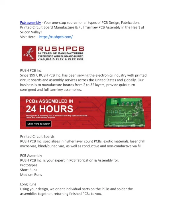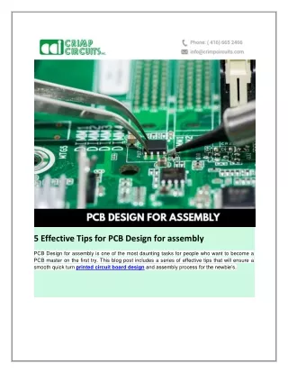
5 Effective Tips for PCB Design for assembly
50 likes | 79 Views
PCB Designing and assembly is not an easy task for new Designers. Follow these effective tips for PCB Design for assembly to become a PCB master on the first go.

5 Effective Tips for PCB Design for assembly
E N D
Presentation Transcript
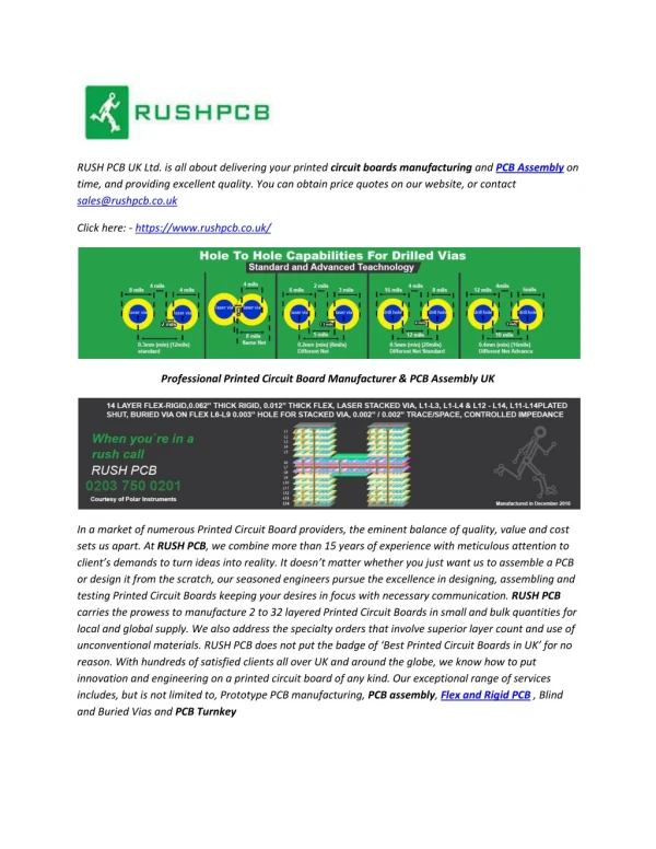
5 Effective Tips for PCB Design for assembly PCB Design for assembly is one of the most daunting tasks for people who want to become a PCB master on the first try. This blog post includes a series of effective tips that will ensure a smooth quick turn printed circuit board designand assembly process for the newbie’s.
Want to become a PCB Master on the first try? Follow these effective tips for PCB Design and assembly #Tip 1: Focus on part-to-part spacing Most of the new designers struggle with component-to-component spacing. Placing two components too close to each other can create numerous issues that may result in redesigning and prefabricating which is a time-consuming and expensive affair. PCB masters make the best use of different techniques to avoid the potential issues that could arise from component disarrangement. They design the footprints in the manner that there is always an adequate gap between the component boundaries and component shapes do not overlap each other. Also, make sure that PCB Design for Assembly Guidelines, component rules and requirements, and proximity regulations have been well-established while designing software for PCB Designing. #Tip 2: Choose components during the design phase It is always advisable to choose the components early during the PCB designing phase. This helps to ensure that there is no discrepancy between the actual PCB design and components assembled. A PCB Designer may take the help of PCB circuit designer and engineers to manage the component space and sizes, higher are your chances to execute the PCB Designing process hassle-free.
#Tip 3: Select the appropriate package size Effective communication between the PCB Designing team and electrical engineer during the early layout stages may outrange severe complications that could occur during PCB assembly. The designer should scrutinize the PCB Designing parts and should recommend component sizes- larger or smaller based on the printed circuit board design space. Choosing the component sizes at the early phase will help in avoiding unnecessary delays during the assembly process. Finally, it’s vital to select the relevant package size during the PCB designing phase. If you have good reasons for choosing a smaller package, go for it otherwise choose bigger options. After selecting the appropriate package size, you can start selecting the components in the similar density category.
#Tip 4: Keep your Bill of Materials (BOM) updated while PCB designing A Bill of Materials (BOM) is a crucial aspect of both PCB Designing and Assembly. Issues in BOM can keep the project on hold until the issues are solved by the engineer. That’s why it is recommended to review your BOM whenever there is a change in printed circuit board design. Do not forget to update the BOM with correct description, part number and component values whenever you add new components to your schematic in the PCB Designing process Recommended format for Bill of Materials (BOM) ●Manufacturer’s name ●Complete manufacturer’s part number ●Complete Part Description ●Per Board Quantity ●Reference designators, separated by commas ●Distributor’s name ●Distributor’s part number #Tip 5: Examinine footprint development Component footprints are also an important aspect of layout design. A PCB Master has to ensure that their footprints are built correctly as per the recommended land pattern in the datasheet. To label the right part and its land pattern, it’s crucial to use the numbering key accurately from the datasheet to avoid the situations of redesigning and re-fabricating boards.
Become a PCB Assembly master by following the above-mentioned PCB Design for Assembly tips. Looking for the best PCB Manufacturers in Canada, feel free to contact us! Read more: https://www.crimpcircuits.com/blog/5- effective-tips-for-pcb-design-for-assembly/