Download

1 / 23
230 likes | 377 Views
The International Technology Roadmap for Semiconductors Overall Roadmap Technology Characteristics (ORTC) Overview. 07/24/02 Alan Allan / Intel Corporation. Key Messages.

E N D
The International Technology Roadmap for Semiconductors Overall Roadmap Technology Characteristics (ORTC) Overview 07/24/02 Alan Allan / Intel Corporation
Key Messages • NO CHANGES to the 2002 ORTC Scaling targets and Chip Size models – First Time Since 1994 NTRS! • Economics (Chip Size) OK through 2004 • Performance (Frequency) OK through 2004 • Density (Functionality) OK through 2004 • But Remember: 1995-2001 2-year Scaling Node Rate… • …And Trends Slip from Historical Rates after 2005 • Room for Improvement in 2003: • Clarification of “Node” and “Production” Definitions; • Watch for Evidence of Industry Acceleration in 2003
Production Definition
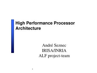
Production Ramp-up Model and Technology Node 100M 200K Development Production 10M 20K 1M 2K Volume (Parts/Month) Alpha Tool Beta Tool Production Tool 100K Volume (Wafers/Month) 200 10K First Two Companies Reaching Production 20 First Conf. Papers 1K 2 0 12 24 -24 -12 Months Source: 2001 ITRS - Exec. Summary
10 10 For 1995-1999 W.P.C.= Total Worldwide Wafer Production Capacity (Relative Value) W.P.C. W.P.C. W.P.C. W.P.C. W.P.C. W.P.C. W.P.C. W.P.C. W.P.C. W.P.C. W.P.C. W.P.C. >0.7 mm 0.4-0.7 mm <0.4mm Sources: 1995 to 1999: SICAS 2000: Yano Research Institute& SIRIJ 1 1 For 2000 Feature Size of Technology Feature Size (Half Pitch) (mm) >0.8 mm 0.5-0.8 mm 0.35-0.5 mm 0.25- 0.35 mm 0.2 - 0.25 mm 0.18 - 0.2 mm <0.18 mm 0.1 0.1 ITRS Technology Node 0.01 0.01 1995 1995 2005 2005 1996 1996 1997 1997 1998 1998 1999 1999 2000 2000 2001 2001 2002 2002 2003 2003 2004 2004 Year Year Source: 2001 ITRS - Exec. Summary Technology Node vs Actual Wafer Production Capacity
Scaling – Technology Nodes
S=0.7 [0.5x per 2 nodes] Pitch Gate MOS Transistor Scaling(1974 to present)
Poly • Pitch • Metal • Pitch (Typical MPU/ASIC) (Typical DRAM) Source: 2001 ITRS - Exec. Summary Half Pitch (= Pitch/2) Definition
2001 ITRS – (No Changes for 2002 Update)SCALING Timing Highlights • Technology Node and Industry Pace: The DRAM Half-Pitch (HP) on a 3-year-cycle trend after 130nm/2001 • The MPU/ASIC HP remains on a 2-year-cycle trend until 90nm/2004, and then remains equal to DRAM HP (3-year cycle) • The MPU Printed Gate Length (Pr GL ) and Physical Gate Length (Ph GL) will be on a 2-year-cycle until 45nm and 32nm, respectively, until the year 2005 • The MPU Pr GL and Ph GL will proceed parallel to the DRAM/MPU HP trends on a 3-year cycle beyond the year 2005 • The ASIC/Low Power Pr/Ph GL is delayed 2 years behind MPU Pr/Ph GL • ASIC HP equal to MPU HP
[3-Year Node Cycle] [Node = DRAM Half-Pitch (HP)] [MPU Gate Length Cycle (GL)]: [2-year cycle] [3-year cycle] [MPU HP/GL Cycle]: [3-year cycle] 2001 ITRS ORTC Node Tables – w/Node Cycles
Table 4c Performance and Package Ch ips: Frequency On - Chip Wiring Levels — Near - Term Years 2001 2002 2003 2004 2005 2006 2007 Y P EAR OF RODUCTION 130 115 100 90 80 70 65 DRAM ½ Pitch (nm) 150 130 107 90 80 70 65 MPU/ASIC ½ Pitch (nm) 90 75 65 53 45 40 35 MPU Printed Gate Length (nm) Chip Frequency (MHz) 65 53 45 37 32 28 25 MPU Physical Gate Length (nm) 1,684 2,317 3,088 3,990 5,173 5,631 6,739 On chip local clock - Chip - to - board (off - chip) speed 1,684 2,317 3,088 3,990 5,173 5,631 6,739 (high - performance, for peripheral buses)[1] 7 8 8 8 9 9 9 Max imum number wiring levels — maximum 7 7 8 8 Maximum number wiring levels — minimum [MPU Gate Length Cycle (GL)]: 8 9 9 [2-Yr GL Cycle; then 3-Yr] Table 4d Performance and Package Chips: Frequency, On - Chip Wiring Levels — Long - term Years 2010 2013 2016 Y P EAR OF RODUCTION 45 32 22 DRAM ½ Pitch ( nm) 45 32 22 MPU/ASIC ½ Pitch (nm) 25 18 13 MPU Printed Gate Length (nm) 18 13 9 MPU Physical Gate Length (nm) Sources: 2001 ITRS ORTC Chip Frequency (MHz) 11,511 19,348 28,751 On chip local clock - Chip - to - board (off - chip) speed 11,511 19,348 28,751 (high - performance, for peripheral buses)[1] 10 10 10 Maximum number wiring levels — maximum [3-year cycle] 9 9 10 Maximum number wiring levels — minimum 2001 ITRS ORTC MPU Frequency Tables – w/Node Cycles
MPU Clock Frequency Actual vs ITRS Historical <- > 1999 ITRS 2001 ITRS 100,000 2X / 4 Years 10,000 Actual Scaling Acceleration, Or Equivalent Scaling InnovationNeeded to maintain historical trend 1,000 Frequency (MHz) 2X / 2½ Years 100 MPU Clock Frequency Historical Trend: Gate Scaling, Transistor Design contributed ~ 17-19%/year Architectural Design innovation contributed additional ~ 21-13%/year 2X / 2 - 2½ Years 10 1 1980 1985 1990 1995 2000 2005 2010 2015 28 Sources: Sematech, 2001 ITRS ORTC
DRAM Cell Area History / 2001 ITRS Model DRAM Cell Area Historical Actual <- > 2001 ITRS History <-- 2000 --> F'cast 10 1 Mb 0.35x / 3 Years –29%/yr Actual Scaling Acceleration, Or Equivalent Scaling InnovationNeeded to maintain historical trend (est.) CAF (A) = 31 = 31/1.0^2 29 (per 1 FEP) 4 Mb 16 Mb CAF (A) CAF (A) 64 Mb = 22 = = 16 = CAF (A) 11/.71^2 4.0/.5^2 = 11 = 26 (per 21 (per 1.3/.35^2; FEP) FEP) .71/.25^2 Cell Area (u2) 0.1 16->10 (per FEP) 128/256Mb 512Mb CAF (A) = 8.0 = DRAM Cell Size Historical Trend: Half-Pitch Scaling, contributed ~ .5x / 3 years [(.7x)^2] Cell Design innovation contributed additional ~ .7x / 3 years .35/.21^2; .26/.18^2 1Gb / 2Gb 10 -> 8 (per FEP) CAF (A) = 6 0.01 4Gb / 8Gb CAF (A) = 6 16Gb / 32Gb CAF (A) = 4 0.001 1986 1989 1992 1995 1998 2001 2004 2007 2010 2013 2016 64 Gb/128Gb Sources: Sematech, 2001 ITRS ORTC Year CAF (A) = 4
Chip Size Trends
(Cell Array Area / Chip Size) x 100 = Cell Array Efficiency (%): Chip Size = (A x f 2 x Nbits)/CAE Cell Array Area = Cell Area x number of bits (2 n) f 2 Cell Area = Cell Area Factor (A) x f 2 ; f = technology node (half-pitch) feature size; Example: Cell Area = 2x4 x f 2 = 8 f 2 Chip Size Model Calculation Illustration - DRAM
MPU Chip size (mm2) – Historical Trends vs 2001 ITRS Model* 1000 800mm2 Litho Field Size 286mm2 2 per Field Size 572mm2 Litho Field Size HP MPU 310mm2 CP MPU 140mm2 100 CP Shrink 70mm2 * ITRS Design TWG MPU Transistors/Chip Model: ~2x/Node = 2x/2yrs from 1999 - 2001; then 2x/3yrs from 2001- 2016 *1999 Leading-Edge .18u CP MPU: 512KB (28Mt [58.3%] x 1.18u2/t = 34mm2) + 20Mt Logic x 5.19u2/t = 104mm2 + 2mm2 OH= 106mm2 = Total 48Mt x ave 2.92u2/t = 140mm2 *1999 Leading- Edge .18u HP MPU: 2MB (113Mt [81.9%] x 1.18u2/t = 135mm2) + 25Mt Logic x 5.19u2/t = 130mm2 + 45mm2 OH= 310mm2 = Total 138Mt x ave 2.25u2/t = 310mm2 10 1980 1985 1990 1995 2000 2005 2010 2015 2020
ITRS 2001 “Moores Law” Targets: DRAM: 2x/2.5yrs; 1.05x/yr Chip Size MPU: 2x/node = 2x/3years; FLAT Chip Size Density Trends (bits/cm2, t/cm2) – ITRS / ORTC
Key Messages • NO CHANGES to the 2002 ORTC Scaling targets and Chip Size models • Economics (Chip Size) OK through 2004 • Performance (Frequency) OK through 2004 • Density (Functionality) OK through 2004 • But Remember: 1995-2001 2-year Scaling Node Rate… • …And Trends Slip from Historical Rates after 2005 • Room for Improvement in 2003: • Clarification of “Node” and “Production” Definitions; • Watch for Evidence of Industry Acceleration in 2003
3-yr Node Cycle vs 2-yr 0.89/yr 0.95/yr 0.71/yr 0.74/yr 2001 ITRS DRAM Model Trend Analysis [Cell Design Improvement Factor]
2001 ITRS DRAM Model Trend Analysis (cont.) 1.26/yr 1.41/yr 0.71/yr 1.34/yr 1.59/yr 1.47/yr 0.74/yr
1994 NTRS - .7x/3yrs Log Half-Pitch Actual - .7x/2yrs 0.7x 0.7x Linear Time 0.5x N N+1 N+2 Scaling Calculator + Node Cycle Time: 250 -> 180 -> 130 -> 90 -> 65 -> 45 -> 32 -> 22 -> 16 Node Cycle Time (T yrs): *CARR(T) = [(0.5)^(1/2T yrs)] - 1 CARR(3 yrs) = -10.9% CARR(2 yrs) = -15.9% * CARR(T) = Compound Annual Reduction Rate (@ cycle time period, T) Source: 2001 ITRS - Exec. Summary