Download
1 / 15
150 likes | 377 Views
Circuit Modeling of Non-volatile Memory Devices. Introduction to NVM Capacitor sub-circuit and sense model Extensions: Program/Erase, 2-bit storage, reliability. M. Sadd and R. Muralidhar. NVM operates with processes that normally cause failure:.

E N D
Circuit Modeling of Non-volatile Memory Devices • Introduction to NVM • Capacitor sub-circuit and sense model • Extensions: Program/Erase, 2-bit storage, reliability M. Sadd and R. Muralidhar
NVM operates with processes that normally cause failure: Need to model effects that are minimized in most other devices!
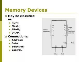
Flash Cell Over-view Flash Cell most common type of NVM: Control Gate ONO Layer Floating Gate Tunnel Oxide The memory becomes “Flash” when organized in an array with “block” erase: NOR Array:
Flash Cell Operations • Operation: • Sense • Program • Erase • Retention • Model Needs to describe: • Variable Threshold voltage • HCI or Tunneling • Tunneling • Charge loss
Flash Sense Operation Memory senses the Vt shift from stored charge: Basic sense circuit:
Flash Sense Model • Simple Approach Separate models for program/erase Vt • More flexible sub-circuit:
Flash Sense Model • Charge stored on floating node: • QFG ~ Cmos Vfg + Cfs Vfg + Cfd(Vfg- Vd) + Ccg(Vfg-Vcg) • Define coupling ratios: • g = Ccg/ (Ccg + Cmos + Cfd+ Cfs) • d = Cfd/ (Ccg + Cmos + Cfd+ Cfs) • Then, • VT ~ -QFG/Ccg+ (1/ g ) VT,FG + (d / g ) Vd • Charge of floating node shifts Vt • Drain coupling to floating gate introduces “DIBL” • Typically g = 0.5-0.75 and d ~ 0.1
Sense Model: Extraction Vg Vd • Extract base MOSFET model by accessing floating gate • Compare to bit-cell to obtain coupling capacitances Vg Vd • Requires comparison of two devices subject to mis-match errors • Extraction with bit-cell alone (e.g. ref) requires erase or program model
Flash Sense Model: Use • Model may only be used for transient simulation • Example: Generating an Id-Vg curve • Ramp Drain from 0 to Vd • Ramp Gate from 0 to Vg • Compute Idrain • Idrain vs. Vgate Ramp slow enough that transient currents (C dV/dt) ~ 0 • Not restrictive: Model used mainly for timing
Flash Sense Model: DC Model May build a DC Flash model: Solve for Floating node potential for capacitor sub-circuit model • See: • Y. Tat-Kwan, et. al. IEDM Tech Dig. p. 157 (1994) • L. Larcher, et. al.IEEE Trans. Elec. Dev., 49 p. 301(2002) Voltage source sets Vfg such that charge QFG is conserved
Flash Program/Erase Model • Time scales: • Read ~ 10 ns • Program ~ 1 s • Erase ~ 100 ms • Retention ~ 10 Years • Read tightest timing, so most need for circuit simulation • Program/Erase May need a circuit model (multi-level storage) Most models add non-linear resistor or current source:
Charge-Trapping NVM Scaled NVM devices charge trapping in a layer of: Nitride (SONOS): Nano-crystals: • Advantages: • Reliability (resistant to defects) • Reduced program/erase voltage • Avoids drain coupling “DIBL”
Charge-Trapping NVM: 2 Bit Storage Two bits may be stored: One each above source or drain: For large Vd charge over source barrier affects charge more than over drain A simple circuit model: Two reads (forward & reverse) can store 4 states:
Reliability Model Non-linear current source model charge loss: • Integrate in log(t) • dQ/d(log(t)) = t dQ/dt = t Itunnel(V) • May calculate long-time loss: Physics of charge loss (tunneling) is lumped into the non-linear current source
Summary • Capacitor sub-circuit foundation for flash model • Appropriate for timing simulation • May be augmented to model: • Program and erase • Reliability (charge loss or gain) • Device asymmetry (2-bit storage)