計算機アーキテクチャ演習第 6 回 PICO の Verilog 記述その2
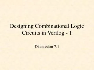
計算機アーキテクチャ演習第 6 回 PICO の Verilog 記述その2. 慶応大学 天野. MUX. MUX. MUX. MUX. MUX. PICO の構成(前期の図を若干変更). regc. aluout. outc. op. pc. ir. com. op2. ALU. op. 110 001. alubin. aluain. Expander. ‘2’. regb. op2. rega. dest. adrA. src. adrB. idata. regfile. ddatain. ddataout.


計算機アーキテクチャ演習第 6 回 PICO の Verilog 記述その2
E N D
Presentation Transcript
計算機アーキテクチャ演習第6回PICOのVerilog記述その2計算機アーキテクチャ演習第6回PICOのVerilog記述その2 慶応大学 天野
MUX MUX MUX MUX MUX PICOの構成(前期の図を若干変更) regc aluout outc op pc ir com op2 ALU op 110 001 alubin aluain Expander ‘2’ regb op2 rega dest adrA src adrB idata regfile ddatain ddataout we_ Instruction Memory Data Memory iadr dadr
前回の演習 • JMP命令を付け加える assign brinst = (op == BNEZ) | (op == BEQZ)| (op==JMP); assign pcset = ( (rega == 16'h0000)&(op == BEQZ)| (rega != 16'h0000)& (op == BNEZ)| (op==JMP) ); assign aluina = (stat[RF_BIT] | brinst) ? pc : rega; assign imm16 = ((op[4:3] == 2'b00 & op != ROP) | brinst | op == LDLI | op == LDHI) ; assign aluinb = stat[RF_BIT] ? 16'h0002 : op==JMP ? { {5{ir[10]}},ir[10:0]}: imm16 ? { {8{ir[7]}}, ir[7:0] } : op == LDHI ? {ir[7:0],8'h00} : regb; 挿入場所に注意
出力オリエンテッドな記述の問題点 • それぞれの出力に関して記述する • 記述が分散的になる • 例えばJMP命令を取り付けるのにも、色々な所をいじる必要がある • もっと、「XX命令の時はYYをする」という感じに書けないだろうか? • 入力オリエンテッド、多入力、多出力の書き方
Function文の利用 本来、Function文は単一出力用だが、無理やり複数出力を扱うことが可能 function [34:0] allgen; input [StateNum-1:0] stat; input [Opcode-1:0] op, op2; input [DataBus-1:0] rega,regb; begin case(stat) RF: allgen = {ADDOP, pc, 16'h0002}; EX: case (op) BNEZ: allgen = {ADDOP, pc,{{8{ir[7]}},ir[7:0]}}; BEQZ: allgen = {ADDOP, pc,{{8{ir[7]}},ir[7:0]}}; LDLI: allgen = {THB, 16'bx,{{8{ir[7]}}, ir[7:0]}} ; LDHI: allgen = {THB, 16'bx,{ir[7:0],8'b0}} ; ROP: allgen = {op2[2:0], rega,regb} ; default: allgen = {op[2:0], rega,{{8{ir[7]}}, ir[7:0]}} ; endcase default: allgen = {op2[2:0], rega,regb}; endcase end endfunction assign {com, aluina,aluinb} = allgen(stat, op, op2, rega, regb); ALUのコマンド、入力を同時に設定
命令単位の記述へ function [35:0] allgen; input [StateNum-1:0] stat; input [Opcode-1:0] op, op2; input [DataBus-1:0] rega,regb; reg azero; begin azero = (rega==16'b0); case(stat) RF: allgen = {Disable,ADDOP, pc, 16'h0002}; EX: case (op) BNEZ: allgen = {~azero,ADDOP, pc,{{8{ir[7]}},ir[7:0]}}; BEQZ: allgen = {azero, ADDOP, pc,{{8{ir[7]}},ir[7:0]}}; LDLI: allgen = {Disable,THB, 16'bx,{{8{ir[7]}}, ir[7:0]}} ; LDHI: allgen = {Disable,THB, 16'bx,{ir[7:0],8'b0}} ; ROP: allgen = {Disable,op2[2:0], rega,regb} ; default: allgen = {Disable,op[2:0], rega,{{8{ir[7]}}, ir[7:0]}} ; endcase default: allgen = {Disable,op2[2:0], rega,regb}; endcase end endfunction assign {pcset, com, aluina,aluinb} = allgen(stat, op, op2, rega, regb); wireが使えないのでregを使う→前前回のバレルシフタ要修正 if文を使ってもいい
Function文を使う場合の注意 • 入力は、指定しないとグローバル変数とマッチしてしまうので注意、必ず指定すること • 出力のビット数と代入が必ず一致するように注意、往々にしてズレる。 • regで中間出力を定義できるが、あまり複雑にしない方が良い。 • 関連のあるものだけをまとめるのが無難。あまり多数の出力を一つのFunctionで扱わない
always文の書き方 reg pcset; reg [ComNum-1:0] com; reg [DataBus-1:0] aluina, aluinb; always @(stat or op or op2 or rega or regb) begin case文 if文など end reg文だが、レジスタではなく、always文の出力 waiting list 入力を全て書く 全ての組み合わせで、 全ての出力を定義する
always文の利用 reg pcset; reg [ComNum-1:0] com; reg [DataBus-1:0] aluina, aluinb; always @(stat or op or op2 or rega or regb) begin case(stat) RF: begin pcset = 0; com = ADDOP; aluina = pc; aluinb = 16'h0002; end EX: case (op) BNEZ: begin if(rega!=16'b0) pcset = Enable; else pcset = Disable; com = ADDOP; aluina = pc; aluinb = {{8{ir[7]}},ir[7:0]}; end BEQZ: begin if(rega==16'b0) pcset = Enable; else pcset = Disable; com = ADDOP; aluina = pc; aluinb = {{8{ir[7]}},ir[7:0]}; end LDLI: begin pcset =Disable; com=THB; aluina = 16'bx; aluinb = {{8{ir[7]}}, ir[7:0]} ; end LDHI: begin pcset =Disable; com=THB; aluina = 16'bx; aluinb = {ir[7:0],8'b0} ; end ROP: begin pcset =Disable; com=op2[2:0]; aluina= rega; aluinb = regb; end default: begin pcset =Disable; com=op[2:0]; aluina= rega; aluinb = {{8{ir[7]}}, ir[7:0]} ; end endcase default: begin pcset =Disable; com=op2[2:0]; aluina= rega; aluinb = regb; end endcase end
memory.v module memory (clk,reset_,iaddr,daddr,dmwe,ddataout,idata,ddatain); `include "pico.h" input clk; input reset_; input [AddrBus-1:0] iaddr; // Instruction Addr to I-Memory input [AddrBus-1:0] daddr; // Data Addr to D-Memory input [DataBus-1:0] ddataout; // Write Data to D-Memory input dmwe; // D-Memory Write Enable output [DataBus-1:0] idata; // Instruction Data from I-Memory output [DataBus-1:0] ddatain; // Read Data from D-Memory reg [DataBus-1:0] imem [MemSize-1:0]; reg [DataBus-1:0] dmem [MemSize-1:0]; assign idata = imem[iaddr[8:1]]; assign ddatain = dmem[daddr[8:1]]; always @ ( posedge clk ) begin if ( dmwe == Enable ) begin dmem[daddr[8:1]] <= ddataout; end end initial begin $readmemb ("test.prg",imem); $readmemh ("test.dat",dmem); end endmodule 256に設定してある ファイルから読込み readmemb:2進数 readmemh:16進数
test.prgとtest.datの例 11100_001_00000000 // LDLI r1,#0 00000_010_001_01000 // LD r2,(r1) 00110_001_00000010 // ADDI r1,#2 00000_011_001_01000 // LD r3,(r1) 11100_100_00000000 // LDLI r4,#0 00000_100_010_00110 // ADD r4,r2 00111_011_00000001 // SUBI r3,#1 01001_011_11111010 // BNEZ r3,-6 00000_001_100_01001 // ST (r1),r4 01010_011_11111110 // BEQZ r3,-2 test.prg 0002 0003 0000 test.dat
テストベンチ(PICOとメモリの接続) `timescale 1ns/1ps module test; `include "pico.h" reg clk; reg reset_; wire [DataBus-1:0] idata; // Instruction Data from I-Memory wire [DataBus-1:0] ddatain; // Read Data from D-Memory wire [AddrBus-1:0] iaddr; // Instruction Addr to I-Memory wire [AddrBus-1:0] daddr; // Data Addr to D-Memory wire [DataBus-1:0] ddataout; // Write Data to D-Memory wire dmwe; // D-Memory Write Enable bpico16 pico (.clk( clk ),.reset_( reset_ ),.idata( idata ),.ddatain( ddatain ), .iaddr( iaddr ),.daddr( daddr ),.ddataout( ddataout ),.dwe( dmwe ) ); memory memory (.clk( clk ),.reset_( reset_ ),.iaddr( iaddr ),.daddr( daddr ), .dmwe( dmwe ),.ddataout( ddataout ),.idata( idata ),.ddatain( ddatain ) );
テストベンチ(クロックとリセット) parameter STEP = 100; always # ( STEP / 2 ) clk <= ~clk; initial begin clk <= 1'b0; reset_ <= Enable_; # ( STEP ) reset_ <= Disable_; # ( STEP * 100 ); $finish; end
テストベンチ(表示部) always @( negedge clk ) begin $display( "stat:%b rfpc:%x rfir:%x r:%x %x %x %x %x %x %x %x", pico.stat, pico.pc, pico.ir, pico.reg0.rfile[0], pico.reg0.rfile[1], pico.reg0.rfile[2], pico.reg0.rfile[3], pico.reg0.rfile[4], pico.reg0.rfile[5], pico.reg0.rfile[6], pico.reg0.rfile[7]); end initial begin $dumpfile("pico.vcd"); $dumpvars(0,pico); end endmodule 状態、pc, ir, register fileを表示 gktwave用のデータ格納ファイル 0nsからpicoモジュールのデータ収集
ikarus verilogの利用法 コンパイル iverilog test.v bpico.v memory.v • pico.h,test.prg,test.datを同じディレクトリに入れておく または iverilog –out ファイル名 test.v bpico.v memory.v この時点でエラーチェックは行われる 実行 vvp a.out または vvp ファイル名
波形を見る テストベンチで指定したファイル名 gtkwave pico.vcd signal search -> Signal Search Hierarchyをクリック Signal Search Hierarchy windows中のモジュール名をクリック 表示したい信号名をクリックしてAppend Wave window中に波形が表れる
今日の演習 JMP X PC<-PC+0x100 01111 00100000000 Jump Function文を使ったもの、always文を使ったものの好きな方についてJMP命令を付け加えよ。
11/15、11/22の演習 bpico.v, test.v, memory.v, pico.h, test.prg, test.datをwebから取ってくる • test.prgを改造し、1からmまでの和を求めるプログラムを作り、動作を確認せよ。mは、0番地または1番地のデータを用いよ。 • bpico.vを改造し、JMPおよびJR命令を付け加えよ。test.prgを改造してテスト用プログラムを作り動作を確認せよ • bpico.vではなく、function文を使ったbpicof.v, always文を使ったbpicoa.vを使っても良い この間と同じグループで良い 11/29までに、授業webに1のtest.prgと2のbpico.vを別々に提出のこと