Sourcing and Sinking Inputs
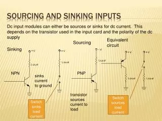
Sourcing and Sinking Inputs. Dc input modules can either be sources or sinks for dc current. This depends on the transistor used in the input card and the polarity of the dc supply. Equivalent circuit. Sourcing. Sinking. NPN. PNP. sinks current to ground.


Sourcing and Sinking Inputs
E N D
Presentation Transcript
Sourcing and Sinking Inputs Dc input modules can either be sources or sinks for dc current. This depends on the transistor used in the input card and the polarity of the dc supply Equivalent circuit Sourcing Sinking NPN PNP sinks current to ground transistor sources current to load Switch sources load current Switch sinks load current
Sourcing and Sinking OutputModules positive universal Common universal Sinking Connections Sourcing Connections
Relationship Between I/O Hardware and Memory Field I/O device is considered load. Must provide sources of potential for I/O To voltage source Memory Map I/O points mapped to memory by PLC software. Users must specify address when programming. Determined by I/O hardware address Output Load Output Module Status Word
PLC Data File Structures Typical structure Allen-Bradley SLC500 Series Memory structure System Memory Application memory ROM holds PLC Operating system RAM Holds user programs and data files I/O maps, programs battery back-up
PLC Data File Structures AB SLC 500 Data File Identifiers File ID number 0 Output Image 1 Input Image 2 Status 3 Bit 4 Timer 5 Counter 6 Control 7 Integer 8 Reserved 9 Network Comm. 10-255 User defined Bit, timer, counter, integer data defined by user
15 14 13 12 11 10 9 8 7 6 5 4 3 2 1 0 addr. PLC Data File Structures File 0 - Output image single memory words Slot address Unused 0 1 0 0 0 1 1 0 O:1 O:2 Point Map O:5 Address depends on slot location of the Output card and number of points
15 14 13 12 11 10 9 8 7 6 5 4 3 2 1 0 addr. Output image File x O:2 Invalid x O:5 x O:6 Invalid x O:7 Each card assigned a word, unused bits are not addressable PLC has an 16 output card in slot 2 An 8 output card in slot 5 A 16 output card in slot 6 An 8 output card in slot 7
15 14 13 12 11 10 9 8 7 6 5 4 3 2 1 0 addr. INPUT image File File 1 - Input image single memory words Slot address I:0 I:3 I:4 Each card assigned a word, unused bits are not addressable Address depends on slot location of the input card and number of points. Similar to Output map.
PLC Data File Structures File 2 - Processor Status File Contains information about how PLC and its operating system is functioning Typical Information monitoring and clearing hardware and software faults setting of watchdog timer value runtime errors I/O errors average scan times
PLC Data File Structures File 3 - The Bit File Bit files used to represent control relays that were used in electromechanical systems. Word identifier Addressing bit data type Data Type (Bit) Bit identifier B3:n/b File ID Number Example: For the following memory map 12 7 5 3 Determine the bit value associated with the addresses Addresses Bit value B3:0/5 B3:1/7 B3:2/12 B3:3/3 1 1 0 0
15 14 13 12 11 10 9 8 7 6 5 4 3 2 1 0 addr. PLC Data File Structures Identifying individual bits B3:0 1 B3:1 B3:2 0 B3:3 B3:1/9 B3:2/8
15 14 13 0 EN TT DN INTERNAL USE ONLY 0 Preset Value (PRE) 1 Accumulated Value (ACC) 2 PLC Data File Structures Timer file structure and addressing File 4 - Timers. Each timer requires 3 words of data file Addressable Bits EN - timer enabled bit TT - timer timing bit DN - timer done bit Word 0 - control word I/O bits and Internal control Word 1 - preset value Word 2 - accumulated value Data Structure is the same for on-delay and off-delay timers
15 14 13 0 EN TT DN INTERNAL USE ONLY 0 Preset Value (PRE) 1 Accumulated Value (ACC) 2 Addressing Timer File Data Sub-elements Examples Tf:e.s/b General form T4:0/15 = T4:0/EN Bit Timer 0; Timer enabled bit Timer file # Default 4 Sub-element T4:1.ACC or T4:1.2 More Examples Element (Timer #) Accumulated value of timer 1 T4:5.ACC/1 T4:2/TT Bit one of accumulated value of Timer 5 Timer timing bit: Timer 2 T4:5/DN Timer 5 done bit T20:2.PRE preset of a timer defined in a user defined file area
15 14 13 0 CU CD DN OV UN UA INTERNAL USE ONLY 0 Preset Value (PRE) 1 Accumulated Value (ACC) 2 Counter File Structure File 5 - Counters Each counter defined by three words in data file Addressable Bits CU - counter up enabled bit CD - counter down enabled bit DN - counter done bit OV - counter overflow bit UN - counter underflow bit UA - update accumulated value (only certain models) PRE - preset value ACC -accumulated value Word 0 - control word I/O bits and Internal control Word 1 - preset value Word 2 - accumulated value
15 14 13 0 CU CD DN OV UN UA INTERNAL USE ONLY 0 Preset Value (PRE) 1 Accumulated Value (ACC) 2 Counter File Structure Examples C5:0/15 = C5:0/CU Counter 0 count up bit C5:1.ACC or C5:1.2 Cf:e.s/b General form Accumulated value of counter Bit C5:5/DN Counter file # Default 5 Sub-element Counter 5 done bit C5:5.ACC/1 Element (Counter #) More Examples Bit 1 of accumulated value of counter 5 C20:2.PRE C5:2/CD Preset of a counter defined in a user defined file area Count down enable bit for counter 2
Control And Integer Files File 6 -Control File Used to store status information for bit operations and stack control operations Integer Data types Signed integer (16 bit): range 0 -+- 32767 Unsigned integer (16 bit) range 0 - 65535 File 7 – Integer Data Addressing Integer values Each integer requires 1 word N7:n Word identifier Integer data Type File ID Number
PLC ladder logic Programming Basic Concepts of PLC Ladder Logic Programming Instructions look like schematic symbols Symbols attached to bit addresses in data maps PLC ladder logic program based on logical “continuity” All input symbols must test true for the output symbol to be true
PLC ladder logic Programming Example system Boolean Equation Could program PLC in verbose language or use ladder logic symbols. Ladder logic used to reduce training of maintenance personnel
Basic PLC Programming Instructions Bit or relay Instructions - test memory location bits Examine if open: XIO examines an input bit for an open condition Examine if closed: XIC examines an input bit for closed condition Bit address Bit address Logic of XIC Logic of XIC
Basic PLC Programming Instructions Output Instructions – Toggle output map bits when rung evaluates true Output Energize (OTE) Instruction becomes true when all instructions to rung become true Bit address Output latch and Output unlatch Output latch become TRUE when input rung instructions become TRUE. Remains TRUE after rung becomes FALSE Output unlatch is used to reset the output latch instruction Bit address Bit address
Basic PLC Programming Instructions More Output Instructions One Shot Instruction Input that allows an event to occur only once during a program scan. Instruction only responds to rising hardware input signal OSR Responds to only FALSE to TRUE transitions
15 14 13 12 11 10 9 8 7 6 5 4 3 2 1 0 addr. Programming Examples Rung Examples: What is the condition of the output instruction (T/F)? O:2 I:0 OTE Instruction 0 1 1746-IA8 1746-OB16 XIC Instruction 0 I:0 Input image table shows a 0 bit, so XIC evaluates to a FALSE I:3 I:4
15 14 13 12 11 10 9 8 7 6 5 4 3 2 1 0 addr. Programming Examples Rung example continued: What is the condition of the output instruction (T/F)? O:2 Rung is FALSE. so OTE is FALSE. This gives 0 in output image I:0 False False 0 1 1746-IA8 1746-OB16 O:0 0 O:2 O:4