Download
1 / 23
230 likes | 312 Views
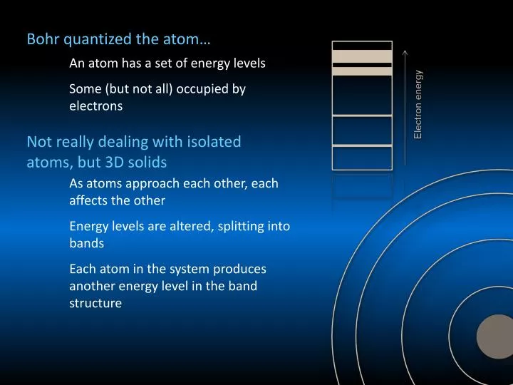
Bohr quantized the atom…. An atom has a set of energy levels Some (but not all) occupied by electrons. Not really dealing with isolated atoms, but 3D solids. As atoms approach each other, each affects the other Energy levels are altered, splitting into bands

E N D
Bohr quantized the atom… An atom has a set of energy levels Some (but not all) occupied by electrons Not really dealing with isolated atoms, but 3D solids As atoms approach each other, each affects the other Energy levels are altered, splitting into bands Each atom in the system produces another energy level in the band structure
Electronic structure of Solids Overlapping levels Outer levels begin to interact gas Broadening of energy levels as atoms approach Degenerate:All electrons in an orbital have the same (lowest) energy Electron energy
Solid Gas E=0 N=5 N=4 N=3 Electron energy N=2 Internuclear distance 3.67Å continuum E=0 Overlapping bands N=4 N=3 Electron energy N=2 Energy bands for solid sodium at internuclear distance of 3.67Å
Solid Gas E=0 N=5 N=4 N=3 Electron energy N=2 Internuclear distance 3.67Å Immediate implication for X-Ray microanalysis… Electron transitions from split levels (bands) will result in photon emission energies that do not reflect the discrete degenerate level…
Conduction band: First empty band above the highest filled band Valence band: Outermost band containing electrons Conduction band Empty band Bandgap Electron energy Outermost band containing elelectrons Valence band Partially full Bandgap Full Bandgap Full nucleus
Transitions from the valence band involved in characteristic X-ray emission will be energy shifted depending on bond lengths, etc. Resulting X-Rays will not be monochromatic These will be Kα X-rays for ultra-light elements Conduction band Empty band Bandgap Electron energy N=2 (L) Valence band Partially full N=1 (K) nucleus
Classification of solids: Conductors Insulators Semiconductors Conductors: Outermost band not completely filled Essentially no band gap overlap lots of available energy states if field is applied Metals and Alkali metals
Insulators: Valence band full or nearly full Wide band gap with empty conduction band Essentially no available energy states to which electron energies can be increased Conduction band Empty Eg Wide bandgap Valence band Full Dielectric breakdown at high potential
Semiconductors: Similar to insulators but narrow band gap At electrical temperatures some electrons can be promoted to the conduction band Most are cubic Diamond FCC (single element) Zinc blende (FCC ZnS) Mark McClure, UNC-Pembroke S Zn Conduction band Almost Empty Conduction band Empty Eg bandgap Valence band Almost Full Valence band Full T > 0K T = 0K Some common band gaps: Element gap (ev) Ge 0.6 Si 1.1 GaAs 1.4 SiO2 9.0
Semiconductors are either intrinsic or extrinsic Intrinsic Semiconductors: Pure state Example: Covalently bonded, tetravalent Si lattice Promotion of an electron to the conduction band leaves “hole” in the valence band = electron-hole pair Apply an electric field and the electron will migrate to + The hole will migrate to – (that is, the electron next to the hole will be attracted to the +, leaving a hole toward -) + - Ec Eg Ev Net propagation of hole
Extrinsic Semiconductors: Doped with impurity atoms p-type n-type n-type Dope Si with something like pentavalent antimony (5 valence electrons) Narrows the band gap relative to Si easy to promote Sb electron Majority carriers are electrons in conduction band Minority carriers are holes in valence band Lattice doped with donor atoms localized energy levels just below conduction band
Ec Ed Ev Si Si lattice with n-type dopant Sb
p-type Dope Si with something like trivalent indium (3 valence electrons) Incomplete bonding with Si Nearby electron from Si can fill hole Majority carriers are holes in the valence band Minority carriers are electrons in the conduction band Lattice doped with acceptor atoms localized energy levels just above valence band
Ec Ea Ev Si Si lattice with p-type dopant In
Ec Eg Ev Valence band Fermi Level: That energy level for which there is a 50% probability of being occupied by an electron Conduction band Ec Intrinsic Eg Ef Ev Valence band Conduction band Ef n-type Recombination Electron-hole pairs not long lasting Electron encountering hole can “fall” into it Free time = microsecond or less
- - - - - - - Depletion width W + + + + + + p n Direction of built-in field Space-charge layers The p-n junction Single crystal of semiconductor Make one end p-type (dope with acceptors) Make the other end n-type (dope with doners) The junction of the two leads to rectification Current only passed in one direction (diode) In the region of the junction Recombination = depletion of region with few charge carriers Results in “built-in” electric field
eV0 - - - - - - - Depletion width W + + + + + + p n Direction of built-in field Space-charge layers Energy band diagram for p-n junction at equilibrium Ecp Ecn Efp Efn Evp Evn Apply eV0 to get diffusion
Energy band diagram for p-n junction – applied forward bias Ecp eV Ecn Efp Efn Evp Evn Depletion width reduced Built-in field reduced Barrier height reduced Diffusion current increased Apply small Vto get diffusion + - - - - - - - - If Vforward = V0 No barrier Pass large current in one direction Depletion width W + + + + + + p n Direction of built-in field Space-charge layers
Energy band diagram for p-n junction – applied reverse bias Ecp eV Evp Ecn Depletion width increased Built-in field increased Barrier height increased - Diffusion current decreased Evn - + - - - - - - - Becomes Capacitor No current passed Depletion width W + + + + + + p n Direction of built-in field Space-charge layers
So: Can use reversed bias p-n junction as voltage regulator Zener diode Voltage too high? Overcome gap energy and pass current Can use forward bias p-n junction for rectification AC → DC transformer Analog-to-digital conversion LED Recombination – “tune” bandgap to achieve photon emission at the required wavelength GaAs (IR) GaInN (blue) GaAsP (red) YAG:Ce (white) Ternary and quaternary compounds allow precise bandgap engineering PIN diode (p and n sections separated by high resistance material) light detection X-ray detection electron detection -Each of these serve to excite electron-hole pairs -Bias properly and get amplification rather than simple propagation
Bipolar transistor = pair of merged diodes - NPN or PNP base base N P N P N P collector emitter collector emitter Three voltages (NPN) Collector = + relative to base (collects electrons) Emitter = - relative to base (emits electrons) Small adjustments of the current on the base results in large changes in collector current. = current amplifier Amplify weak signals Use small currents to switch large ones
Simple optical encoding: Generate sine wave by LED passing ruled slide Phototransistor sees varying light intensity current output varies with base current Diode rectifies AC→DC Square waves Digital output to counter