Download
1 / 26
280 likes | 339 Views
Explore optical reflectance measurements on crystal structures for band structure determination. Learn about dielectric function components and their relation to observable quantities.

E N D
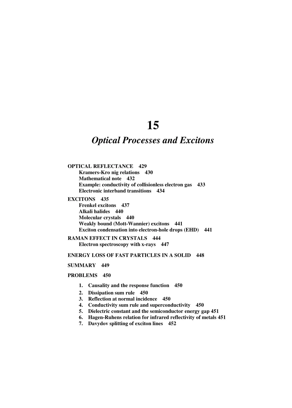
15 Optical Processes and Excitons OPTICAL REFLECTANCE 429 Kramers-Kro nig relations 430 Mathematical note 432 Example: conductivity of collisionless electron gas 433 Electronic interband transitions 434 EXCITONS 435 Frenkel excitons 437 Alkali halides 440 Molecular crystals 440 Weakly bound (Mott-Wannier) excitons 441 Exciton condensation into electron-hole drops (EHD) 441 RAMAN EFFECT IN CRYSTALS 444 Electron spectroscopy with x-rays 447 ENERGY LOSS OF FAST PARTICLES IN A SOLID 448 SUMMARY 449 PROBLEMS 450 1. Causality and the response function 450 2. Dissipation sum rule 450 3. Reflection at normal incidence 450 4. Conductivity sum rule and superconductivity 450 5. Dielectric constant and the semiconductor energy gap 451 6. Hagen-Ruhens relation for infrared reflectivity of metals 451 7. Davydov splitting of exciton lines 452
Raman scattering (generic term): Brillouin scattering when acoustic phonon is involved; polariton scattering when optical phonon is involved. f + for phonon emission (Stokes process) \ - for phonon absorption (anti-Stokes) Electron spectroscopy with x-rays (XPS): incident x-ray photon ejects valence or core electron from solid. Figure X There are many types of experiments in which light interacts with wave like excitations in a crystal. Several absorption processes are illustrated here. 428
CHAPTER 15: OPTICAL PROCESSES AND EXCITONS The dielectric function e(<n, K) was introduced in the preceding chapter to descrihe the response of a crystal to an electromagnetic field (Fig. 1). The dielectric function depends sensitively on the electronic band structure of a crystal, and studies of the dielectric function by optical spectroscopy are very useful in the determination of the overall band structure of a crystal. Indeed, optical spectroscopy has developed into the most important experimental tool for band structure determination. In the infrared, visible, and ultraviolet spectral regions the wavevector of the radiation is very small compared with the shortest reciprocal lattice vector, and therefore it may usually be taken as zero. We are concerned then with the real e' and imaginary e" parts of the dielectric function at zero wavevector; e(a>) = e'M + i€,r((o), also written as e1(w) + ie2M- However, the dielectric function is not directly accessible experimentally from optical measurements: the directly accessible functions are the reflectance R(a>), the refractive index n(n>), and the extinction coefficient K(co). Our first objective is to relate the experimentally observable quantities to the real and imaginary parts of the dielectric function. OPTICAL REFLECTANCE The optical measurements that give the fullest information on the electronic system are measurements of the reflectivity of light at normal incidence on single crystals. The reflectivity coefficient r(o>) is a complex function defined at the crystal surface as the ratio of the reflected electric field E(rcfl) to the incident electric field E(inc): E(ref])/E(inc) = r(io) = p(n>) exp[i0(n>)] , (1) where we have separated the amplitude p((o) and phase 6(a)) components of the reflectivity coefficient. The refractive index n(o)) and the extinction coefficient K{co) in the crystal are related to the reflectivity at normal incidence by n + iK - I n + iK + 1 ’ rW = (2) as derived in Problem 3 by elementary consideration of the continuity of the components of E and B parallel to the crystal surface. By definition, n{w) and K(a>) are related to the dielectric function e(a>) by Ve(o) = n((o) + iKM = N(<o) , (3) 429
430 where N(a) is the complex refractive index. Do not confuse K(a) as used here with the symbol for a wavevector. If the incident traveling wave has the wavevector k, then the y component of a wave traveling in the x direction is Ey(inc) = Elj0 exp[i(kx - at)] . (4) The transmitted wave in the medium is attenuated because, by the dispersion relation for electromagnetic waves, the wavevector in the medium is related to the incident k in vacuum by (n + iK)k: Ey(trans) °c exp {[i[(n + iK)kx — tut]} = exp(~Kkx) exp[i(nkx — at)] . (5) One quantity measured in experiments is the reflectance R, defined as the ratio of the reflected intensity to the incident intensity: R = £*(refl)E(refl)/E*(inc)E(inc) = r+r = p2 . (6) It is difficult to measure the phase 6(a) of the reflected wave, but we show below that it can be calculated from the measured reflectance R(a) if this is known at all frequencies. Once we know both R(ca) and 0(a), we can proceed by (2) to obtain n(a) and K(a). We use these in (3) to obtain e(a) = e'(a) + ien(a), where e'(a) and e"(a) are the real and imaginary parts of the dielectric function. The inversion of (3) gives e(a) = n2 - K2;e”(a) = 2nK . (7) We now show how to find the phase 0(a) as an integral over the reflectance R(a)\ by a similar method we relate the real and imaginary parts of the dielectric function. In this way we can find everything from the experimental R(a). Rramera-Kronig Relations The Kramers-Kronig relations enable us to find the real part of the response of a linear passive system if we know the imaginary part of the response at all frequencies, and vice versa. They are central to the analysis of optical experiments on solids. The response of any linear passive system can be represented as the superposition of the responses of a collection of damped harmonic oscillators with masses Mj. Let the response function a(a) = a'(a) + ia"(a) of the collection of oscillators be defined by xm = a(a)Fw , (8) where the applied force field is the real part of Fw exp(—iat) and the total displacement x = 2 xj is the real part of exp (—iat). From the equation of motion, j Mj(d2/dt2 + pjd/dt + apXj = F ,
15 Optical Processes and Excitons 431 we have the complex response function of the oscillator system: A to + icopj = 2/— a(to) = 2 (9) (caf - to2)2 + to2pf tO j Q)j where the constants /- = l/Mj and relaxation frequencies pj are all positive for a passive system. If a (to) is the dielectric polarizability of atoms in concentration n, then/ has the form of an oscillator strength times nez/m; such a dielectric response function is said to be of the Kramers-Heisenberg form. The relations wc develop also apply to the electrical conductivity <j(to) in Ohms law, ja = We need not assume the specific form (9), but wc make use of three properties of the response function viewed as a function of the complex variable to. Any function with the following properties will satisfy the Kramers-Kronig relations (11): (a) The poles of a(to) are all below the real axis. (b) The integral of a (to)/to vanishes when taken around an infinite semicircle in the upper half of the complex to- plane. It suffices that a (to) —> 0 uniformly as I o>l —> 00. (c) The function a'(to) is even and a"(to) is odd with respect to real to. Consider the Cauchy integral in the form ot(a>) = -jr P [ ^ m J * a(s) ds (10) where P denotes the principal part of the integral, as discussed in the mathematical note that follows. The right-hand side is to be completed by an integral over the semicircle at infinity in the upper half-plane, but we have seen in (b) that this integral vanishes. We equate the real parts of (10) to obtain v x in r «"(*), ij(”<*’'(*) j , r aM = 77PJ_^0)ds=¥P I =lT,dP In the last integral we substitute s for — p and use property (c) that a"(—s) —ad'fy); this integral then becomes 1a”(s) s + to ds and we have, with 2s .9 ~t0 S + tO to
432 the result =|p/; sa”(s) ds . (Ha) This is one of the Kramers-Kronig relations. The other relation follows on equating the imaginary parts of Eq. (10): _i D r j. _ _i J j r *(*) ,1 «(<d) irPJ -n-P[J0s-a.* J0 .s -I- &> ’ whence (lib) These relations are applied below to the analysis of optical reflectance data; this is their most important application. Let us apply the Kramers-Kronig relations to r(cu) viewed as a response function between the incident and reflected waves in (1) and (6). We apply (11) to In r(<o) = In Rm(a>) + id(co) to obtain the phase in terms of the reflectance: (12) In R(s) (13) ds o s2~ (o2 J ( We integrate by parts to obtain a form that gives insight into the contributions to the phase angle: d In R(s) ds (14) 6(a>) =~2tt ds CO Spectral regions in which the reflectance is constant do not contribute to the integral; further, spectral regions s > to and s < o> do not contribute much because the function In I(s + co)/(s — <u)l is small in these regions. Mathematical Note. To obtain the Cauchy integral (10) we take the integral }a(s)(s — a))-1ds over the contour in Fig. 2. The function a(s) is analytic in the upper half-plane, so that the value of the integral is zero. The contribution of segment (4) to the integral vanishes if the integrand a(s)/s —» 0 is faster than Isl-1 as \s\ —> co. For the response function (9) the integrand —> 0 as Isl-3: and for the conductivity cj(s)the integrand —> 0 as Isl-2. The segment (2) contributes, in the limit as u —» 0, f “(s) j . / \ f°mei6d0 . , ^ . _ M ds oc(oj) -= -7na{co) J(2)S Jit Ue9
IS Optical Processes and Excitons 433 Figure 2 Contour for the Cauchy principal value integral. to the integral, where $ = a> + u et9. Thesegments (1) and (3) are by definition the principal part of the integral between —and00. Because the integral over (1) -I- (2) + (3) + (4) must vanish, a(s) , . , , s. - 0)ds = ma{(o) / (15) J(l) J(3) J- as in (10). EXAMPLE: Conductivity of Collisionless Electron Gas. Consider a gas of free electrons in the limit as the collision frequency goes to zero. From (9) the response function is, with/ — 1/m, f ip rrua [ft) 1 1 (16) i7r8((o) a((o) — — —— lim , v ' mat p^0(l) + by the Dirac identity. We confirm that the delta function in (16) satisfies the Kramers-Kronig relation (11a), by which 2 r 8(s) 1 J o s — to ma.j (17) in agreement with (16). We obtain the electrical conductivity cr((o) from the dielectric function e((o) — 1 = 4irPa/E„ — —4rmexJE^ = 4ime2a(o)) , (18) where a(tu) = xJ{—e)Eti> is the response function. We use the equivalence (CGS) <r{a>) = (-tw/4fr)[e(G>) - 1] , (19) for the Maxwell equation can be written either as c curl H — 4ircr(w)E — ixoE or as c curl H = —i(i)e((o)E. We combine (16), (18), and (19) to find the conductivity of a collisionless electron gas: cr'(<o) + ^ . (20) For collisionless electrons the real part of the conductivity has a delta function at o> = 0.
434 Electronic Interband Transitions It came as a surprise that optical spectroscopy developed as an important experimental tool for the determination of band structure. First, the absorption and reflection bands of crystals are broad and apparently featureless functions of the photon energy when this is greater than the band gap. Second, direct interband absorption of a photon fax) will occur at all points in the Bril-louin zone for which energy is conserved: fax) = ec(k) - ev(k) , (21) where c is an empty band and v is a filled band. The total absorption at given a) is an integral over all transitions in the zone that satisfy (21). Three factors unraveled the spectra: • The broad bands are not like a spectral line greatly broadened by damping, but the bands convey much intelligence which emerges when derivatives are taken of the reflectance (Fig. 3); derivatives with respect to wavelength, electric field, temperature, pressure, or uniaxial stress, for example. The spectroscopy of derivatives is called modulation spectroscopy. Figure 3 Comparison of (a) reflectance, (b) wavelength derivative reflectance (first derivative), and (c) electroreflectance (third derivative), of the spectral region in germanium between 3.0 and 3.6 eV. (After data by D. D. Sell, E. O. Kane, and D. E. Aspnes.)
15 Optical Processes and Excitons • The relation (21) does not exclude spectral structure in a crystal, because transitions accumulate at frequencies for which the bands c, v are parallel— that is, at frequencies where Vk[ec(k)-ev(k)]=0 . (22) At these critical points in k space the joint density of states Dc(ev + ha))D0(ev) is singular, according to the same argument we used in (5.37) to show that the density of phonon modes D(o>) is singular when Vka> is zero. • The pseudopotential method for calculating energy bands helps identify the positions in the Brillouin zone of the critical points found in modulation spectra. Band-band energy differences can be calculated with an accuracy as good as 0.1 eV. The experimental results can then be fed back to give improvements in the pseudopotential calculations. EXCITONS Reflectance and absorption spectra often show structure for photon energies just below the energy gap, where we might expect the crystal to be transparent. This structure is caused by the absorption of a photon with the creation of a bound electron-hole pair. An electron and a hole may be bound together by their attractive coulomb interaction, just as an electron is bound to a proton to form a neutral hydrogen atom. The bound electron-hole pair is called an exciton, Fig. 4. An exciton can move through the crystal and transport energy; it does not transport charge Figure 4a An exciton is a bound electron-hole pair, usually free to move together through the crystal. In some respects it is similar to an atom of positronium, formed from a positron and an electron. The exciton shown is a Mott-Wannier exciton: it is weakly bound, with an average electron-hole distance large in comparison with the lattice constant. Figure 4b A tightly-bound or Frenkel exciton shown localized on one atom in an alkali halide crystal. An ideal Frenkel exciton will travel as a wave throughout the crystal, but the electron is always close to the hole.
436 because it is electrically neutral. It is similar to positronium, which is formed from an electron and a positron. Excitons can be formed in every insulating crystal. When the band gap is indirect, excitons near the direct gap may be unstable with respect to decay into a free electron and free hole. All excitons are unstable with respect to the ultimate recombination process in which the electron drops into the hole. Excitons can also form complexes, such as a biexciton from two excitons. We have seen that a free electron and free hole are created whenever a photon of energy greater than the energy gap is absorbed in a crystal. The threshold for this process is ha) > Eg in a direct process. In the indirect phonon-assisted process of Chapter 8 the threshold is lower by the phonon energy hCl. But in the formation of excitons the energy is lowered with respect to these thresholds by the binding energy of the exciton, which may be in the range 1 meV to 1 eV, as in Table 1. Excitons can be formed by photon absorption at any critical point (22), for if Vket = Vket the group velocities of electron and hole are equal and the particles may be bound by their coulomb attraction. Transitions leading to the formation of excitons below the energy gap are indicated in Figs. 5 and 6. The binding energy of the exciton can be measured in three ways: • In optical transitions from the valence band, by the difference between the energy required to create an exciton and the energy to create a free electron and free hole, Fig. 7. • In recombination luminescence, by comparison of the energy of the free electron-hole recombination line with the energy of the exciton recombination line. • By photo-ionization of excitons, to form free carriers. This experiment requires a high concentration of excitons. We discuss excitons in two different limiting approximations, one by Frenkel in which the exciton is small and tightly bound, and the other by Mott and Wannier in which the exciton is weakly bound, with an electron-hole separation large in comparison with a lattice constant. Intermediate examples are known. Table 1 Binding energy of excitons, in meV Data assembled by Frederick C, Brown and Arnold Schmidt.
15 Optical Processes and Excitons 437 Conduction band (effective mass mj Energy gap, E Valence band (effective mass Figure 5 Exciton levels in relation to the conduction band edge, for a simple band structure with both conduction and valence band edges at k = 0. An exciton can have translational kinetic energy. Excitons are unstable with respect to radiative recombination in which the electron drops into the hole in the valence band, accompanied by the emission of a photon or phonons. ) Exciton binding j energy Energy gap 0 Figure 6 Energy levels of an exciton created in a direct process. Optical transitions from the top of the valence band are shown by the arrows; the longest arrow corresponds to the energy gap. The binding energy of the exciton is ECT, referred to a free electron and free hole. The lowest frequency absorption line of the crystal at absolute zero is not Eex, but is Eg — E Frenkel Excitons In a tightly bound exciton (Fig. 4b) the excitation is localized on or near a single atom: the hole is usually on the same atom as the electron although the pair may be anywhere in the crystal. A Frenkel exciton is essentially an excited state of a single atom, but the excitation can hop from one atom to another by virtue of the coupling between neighbors. The excitation wave travels through the crystal much as the reversed spin of a magnon travels through the crystal. The crystalline inert gases have excitons which in their ground states correspond somewhat to the Frenkel model. Atomic krypton has its lowest strong
438 1.2 -Exciton absorption 1.1- • •• *V^\ 1.0- Absorption with formation of free electron-hole pairs S S G C c I- o 0.8 0.7- 0.6L i i i 1.50 1.51 1.52 1.53 1.54 1.55 1.56 Photon energy in eV Figure 7 Effect of an exciton level on the optical absorption of a semiconductor for photons of energy near the band gap Eg in gallium arsenide at 21 K. The vertical scale is the intensity absorption coefficient a, as in Z(x) = J0 exp( —ax). The energy gap and exciton binding energy are deduced from the shape of the absorption curve: the gap Eg is 1.521 eV and the exciton binding energy is 0.0034 eV. (After M. D. Sturge.) atomic transition at 9.99 eV. The corresponding transition in the crystal is closely equal and is at 10.17 eV, Fig. 8. The energy gap in the crystal is 11.7 eV, so the exciton ground state energy is 11.7 — 10.17 = 1.5 eV, referred to a free electron and free hole separated and at rest in the ciystal. The translational states of Frenkel excitons have the form of propagating waves, like all other excitations in a periodic structure. Consider a crystal of N atoms on a line or ring. If Uj is the ground state of atomj, the ground state of the crystal is il*g = u1u2'“UN-luN , (23) if interactions between the atoms are neglected. If a single atom j is in an excited state Vj, the system is described by <Pj = «i* ’ * Uj-\VjUJ+y ■ • * uN . (24) This function has the same energy as the function <pj with any other atom l excited. However, the functions (p that describe a single excited atom and N — 1 atoms in their ground state are not the stationary quantum states of the problem. If there is any interaction between an excited atom and a nearby atom in its ground state, the excitation energy will be passed from atom to atom. The eigenstates will have a wavelike form, as we now show.
IS Optical Processes and Excitons 439 13.0 12.0 11.0 10.0 ha), eV Figure 8 Absorption spectrum of solid krypton at 20 K. (After G. Baldini.) When the hamiltonian of the system operates on the function q>j with the jth atom excited, we obtain ^<Pj = c<Pj + T(<p^i + <pj+1) , (25) where e is the free atom excitation energy; the interaction T measures the rate of transfer of the excitation from j to its nearest neighbors, j — 1 and 7 + 1. The solutions of (25) are waves of the Bloch form: = 2 exp(ijka) <Pj ■ (26) j To see this we let operate on fa: 9% = 2 WVj = 2 ^ [e<Pj + n<Pj-i + <PJ+1)] , (27) J J from (25). We rearrange the right-hand side to obtain Wfa = ^ eiJka[e + T(eika + e^)]^ = (e + 2Tcos ka)fa , (28) j so that the energy eigenvalues of the problem are Ek = e + 2T cos ka , (29)
440 Energy' Figure 9 Energy versus wavevector for a Frenkel exciton, calculated with positive nearest-neighbor transfer interaction T. as in Fig. 9. The application of periodic boundary conditions determines the allowed values of the wavevector k: k = 2irs/Na- s = -|.V, + 1, • • •, - 1 . (30) Alkali Halides. In alkali halide crystals the lowest-energy excitons are localized on the negative halogen ions, as in Fig. 4b. The negative ions have lower electronic excitation levels than do the positive ions. Pure alkali halide crystals are transparent in the visible spectral region, which means that the exciton energies do not lie in the visible, but the crystals show considerable excitonic absorption structure in the vacuum ultraviolet. A doublet structure is particularly evident in sodium bromide, a structure similar to that of the lowest excited state of the krypton atom—which is isoelectronic with the Br~ ion of KBr. The splitting is caused by the spin-orbit interaction. These excitons are Frenkel excitons. Molecular Crystals. In molecular crystals the covalent binding within a molecule is strong in comparison with the van der Waals binding between molecules, so that the excitons are Frenkel excitons. Electronic excitation lines of an individual molecule appear in the crystalline solid as an exciton, often with little shift in frequency. At low temperatures the lines in the solid are quite sharp, although there may be more structure to the lines in the solid than in the molecule because of the Davydov splitting, as discussed in Problem 7.
15 Optical Processes and Excitons 441 Weakly Bound (Mott-Wannier) Excitons Consider an electron in the conduction band and a hole in the valence band. The electron and hole attract each other by the coulomb potential (CCS) U(r) = -e2/er , (31) where r is the distance between the particles and e is the appropriate dielectric constant. (The lattice polarization contribution to the dielectric constant should not be included if the frequency of motion of the exciton is higher than the optical phonon frequencies.) There will be bound states of the exciton system having total energies lower than the bottom of the conduction band. The problem is the hydrogen atom problem if the energy surfaces for the electron and hole are spherical and nondegenerate. The energy levels referred to the top of the valence band are given by a modified Rydberg equation F _ Fye H g 2ftW (CGS) (32) Here n is the principal quantum number and fi is the reduced mass: I = JL + i M m, mh (33) formed from the effective masses me, mh of the electron and hole. The exciton ground state energy is obtained on setting n = 1 in (32); this is the ionization energy of the exciton. Studies of the optical absorption lines in cuprous oxide, Cu20, at low temperatures give results for the exciton level spacing in good agreement with the Rydberg equation (32) except for transitions to the state n = 1. An empirical fit to the lines of Fig. 10 is obtained with the relation u(cm_1) = 17,508 — (800/n2). Taking € = 10, we find /i —0.7 m from the coefficient of 1 /n2.The constant term 17,508 cm-1 corresponds to an energy' gap Eg = 2.17 eV. Exciton Condensation into Electron-Hole Drops (EHD) A condensed phase of an electron-hole plasma forms in Ge and Si when maintained at a low temperature and irradiated by light. The following sequence of events takes place when an electron-hole drop (EHD) is formed in Ge: The absorption of a photon of energy hco > Eg produces a free electron and free hole, with high efficiency These combine rapidly, perhaps in 1 ns, to form an exciton. The exciton may decay with annihilation of the e-h pair with a lifetime of 8 ju-s. If the exciton concentration is sufficiently high—over 1013 cm-3 at 2 K— most of the excitons will condense into a drop. The drop lifetime is 40 /xs, but in strained Ge may be as long as 600 jlis. Within the drop the excitons dissolve into a degenerate Fermi gas of electrons and holes, with metallic properties: this state was predicted by L. V. Keldysh.
442 Photon energy in 2.14 eV 2.12 2.13 2.16 2.15 Figure 10 Logarithm of the optical transmission versus photon energy in cuprous oxide at 77 K, showing a series of exciton lines. Note that on die vertieal axis the logarithm is plotted decreasing upward; thus a peak corresponds to absorption. The band gap Eg is 2.17 eV. (After R W. Baumeister.) ha), in meV Figure 11 Recombination radiation of free electrons ■with holes and of electron-hole drops in Ge at 3.04 K. The Fermi energy in the drop is eF and the cohesive energy of the drop with respect to a free cxciton is </>,. (After T. K. Lo.) Figure 11 shows the recombination radiation in Ge from free excitons (714 meV) and from the EHD phase (709 meV). The width of the 714 meV line is accounted for by Doppler broadening, and the width of the 709 meV line is compatible with the kinetic energy distribution of electrons and holes in a Fermi gas of concentration 2 X 1017cm-3. Figure 12 is a photograph of a large EHD.
15 Optical Processes and Excitons 443 Figure 12 Photograph of an electron-hole drop in a 4 mm disk of pure germanium. The drop is the intense spot adjacent to the set screw on the left of the disk. The photograph is the image of the drop obtained by focusing its electron-hole recombination luminescence onto the surface of an infrared-sensitive camera. (After J. P. Wolfe et al.) Figure 13 Phase diagram for photoexcited electrons and holes in unstressed silicon. The diagram shows, for example, that with an average concentration near 1017 cm-3 at 15 K, a free-exciton gas with saturated-gas concentration of 1016 cm-3 coexists with a (variable) volume of liquid droplets, each with a density of 3 X 1018 cm''3. The liquid critical temperature is about 23 K. Theoretical and experimental values for the metal-insulator transition for excitons are also shown. (From J. P. Wolfe.)
444 Table 2 Electron-hole liquid parameters Courtesy of D. Bimberg. The exciton phase diagram for silicon is plotted in the temperature-concentration plane in Fig. 13. The exciton gas is insulating at low pressures. At high pressures (at the right of the diagram) the exciton gas breaks up into a conducting plasma of unpaired electrons and holes. The transition from exci-tons to the plasma is an example of the Mott transition, Chapter 14. Further data are given in Table 2. RAMAN EFFECT IN CRYSTALS Raman scattering involves two photons—one in, one out—and is one step more complex than the one photon processes treated earlier in this chapter. In the Raman effect a photon is scattered inelastically by a crystal, with creation or annihilation of a phonon or magnon (Fig. 14). The process is identical to the inelastic scattering of x-rays and it is similar to the inelastic scattering of neutrons by a crystal. The selection rules for the first-order Raman effect are a> = (o'±n ; k = k' ±K , (34) where co,k refer to the incident photon; cof,k' refer to the scattered photon; and fi, K refer to the phonon created or destroyed in the scattering event. In the second-order Raman effect, two phonons are involved in the inelastic scattering of the photon. The Raman effect is made possible by the strain-dependence of the electronic polarizability. To show this, we suppose that the polarizability a associated with a phonon mode may be written as a power series in the phonon amplitude u: a = a0 + a\u + a2u2 + • ■ * . (35) If u(t) = uQ cos fit and the incident electric field is E(t) = E0 cos then the induced electric dipole moment has a component ajEoi/o cos cot cos fit = |n1E0M0[cos(o) + fl)t + cos(w — fl)t] . (36)
1S Optical Processes and Excitons 445 Figure 14 Raman scattering of a photon with emission or absorption of a phonon. Similar processes occur with magnons (spin waves). Thus photons at frequencies co + fi and co — fl can be emitted, accompanied by absorption or emission of a phonon of frequency ft. The photon at co — ft is called the Stokes line and that at o> + ft is the anti-Stokes line. The intensity of the Stokes line involves the matrix element for phonon creation, which is just the matrix element for the harmonic oscillator, as in Appendix C: I(co — ft) |{nK + l|u|nK)|2 nK + 1 , (37) where nK is the initial population of phonon mode K. The anti-Stokes line involves phonon annihilation, with a photon intensity proportional to 1(a) + ft) °c l(nK — l)u)nK)f2 nK . (38) Tf the phonon population is initially in thermal equilibrium at temperature T, the intensity ratio of the two lines is /(co + ft) _ (nK) 7(to ~ ft) (tij) + 1 exp (—}iO/kBT) (39) with (nK) given by the Planck distribution function l/[exp(hO/kBT) — 1]. We see that the relative intensity of the anti-Stokes lines vanishes as T —> 0, because here there are no thermal phonons available to be annihilated. Observations on the K = 0 optical phonon in silicon are shown in Figs. 15 and 16. Silicon has two identical atoms in the primitive cell, and there is no electric dipole moment associated with the primitive cell in the absence of deformation by phonons. But ap/ does not vanish for silicon at K = 0, so that we can observe the mode by first-order Raman scattering of light. The second-order Raman effect arises from the term a2u2 in the polarizability'. Inelastic scattering of light in this order is accompanied by the creation of two phonons, or the absorption of two phonons, or the creation of one and the absorption of another phonon. The phonons may have different frequencies. The intensity' distribution in the scattered photon spectrum may be quite complicated if there are several atoms in the primitive cell because of the
446 Figure 15 First-order Raman spectra of the K — 0 optical mode of a silicon crystal observed at three temperatures. The incident photon has a wavelength of 5145 A. The optical phonon frequency is equal to the frequency shift; it depends slightly on the temperature. (After T. R. Hart, R. L. Aggarwal, and B. Lax.) Figure 16 Intensity ratio of anti-Stokes to Stokes lines as a function of temperature, for the observations of Fig. 15 on the optical mode of silicon. The observed temperature dependence is in good agreement with the prediction of Eq. (39): the solid curve is a plot of the function exp (—hd/kBT). Raman shift, cm J Figure 17 Raman spectrum of GaP at 20 K. The two highest peaks are the first-order Raman lines associated with the excitation of an LO phonon at 404 cm-1 and a TO phonon at 366 cm-1. All the other peaks involve two phonons. (After M. V. Hob den and J. P. Russell.)
15 Optical Processes and Excitom 447 corresponding number of optical phonon modes. Second-order Raman spectra have been observed and analyzed in numerous crystals. Measurements on gallium phosphide (GaP) are shown in Fig. 17. Electron Spectroscopy with X-Rays The next degree of complexity in optical processes involves a photon in and an electron out of the solid, as in Fig. 1. Two important techniques are x-ray photoemission from solids (XPS) and ultraviolet photoemission (UPS). In solid state physics they are used in band structure studies and surface physics, including catalysis and adsorption. XPS and UPS spectra can be compared directly with valence band densities of states D(e). The specimen is irradiated with highly monochromatic x-rays or ultraviolet photons. The photon is absorbed, with the emission of a photoelectron whose kinetic energy is equal to the energy of the incident photon minus the binding energy of the electron in the solid. The electrons come from a thin layer near the surface, typically 50 A in depth. The resolution of the best XPS spectrometer systems is less than 10 meV, which permits refined studies of band structure. The valence band structure of silver is shown by Fig. 18, with the zero of energy set at the Fermi level. Electrons in the first 3 eV below the Fermi level come from the 5s conduction band. The strong peak with structure below 3 eV is from the 4d valence electrons. Excitations are also seen from deeper levels, often accompanied by excitation of plasmons. For example, in silicon the 2p electron with a binding energy close to 99.2 eV is observed in replica at 117 eV with single plasmon excitation and at 134.7 eV with two plasmon excitation. The plasmon energy is 18 eV. Figure 18 Valence-band electron emission from silver, after Siegbahn and co-workers.
448 ENERGY LOSS OF FAST PARTICLES IN A SOLID So far we have used photons as probes of the electronic structure of solids. We can also use electron beams for the same purpose. The results also involve the dielectric function, now through the imaginary part of l/e{co). The dielectric function enters as Im{e(co)} into the energy loss by an electromagnetic wave in a solid, but as — Im{l/e(&>)} into the energy loss by a charged particle that penetrates a solid. Consider this difference. The general result from electromagnetic theory for the power dissipation density by dielectric losses is (CGS) & = -f- e • (aD/at) 4tt (40) per unit volume. With a transverse electromagnetic wave Ee ,<ot in the crystal, we have dD/dt = — ico e(o))Ee~twt, whence the time-average power is <3f> = -^{Re{Ee-iQ*}ne{-io)e(a))Ee-ia>t}) 47r = -p- coE2((e”cos cot — e'sin <yf)cos cot) = (joe"{co)E2 , (41) 477077 proportional to e”(co). The tangential component of E is continuous across the boundary of the solid. If a particle of charge e and velocity i; enters a crystal, the dielectric displacement is, by standard texts, (CGS) D(r,f) - -grad (42) r - vt\ because by the Poisson equation it is D, and not E, that is related to the free charge. In an isotropic medium the Fourier component E(co,k) is related to the Fourier component D(co,k) of D(r,f) by E(co,k) = D(a>,k)/e(o>,k). The time-average power dissipation associated with this Fourier component is S^(o),k) = -^-(Re{6_1(ft>,k)L)(n>,k)e_t<0t}Re{— ico D(co,k) e~lC!)'}) 477 COS cot + sill — = t‘°DVk) sin tot\ whence a) | | qD\(o,k) (43)
15 Optical Processes and Excitons 449 Figure 19 e"(o>) for Cu and Au; the bold lines are from energy loss measurements by J. Daniels, and the other lines were calculated from optical measurements by D. Beaglehole, and L. R. Canfield ct al. The result is the motivation for the introduction of the energy loss function —Im(l/e(oj,k)} and it is also a motivation for experiments on energy losses by fast electrons in thin films. If the dielectric function is independent of k. the power loss is = -§|Mm{l/e(6>))]n(fe0iVa>) , (44) where hk0 is the maximum possible momentum transfer from the primary particle to an electron of the crystal. Figure 19 shows the excellent experimental agreement between values of e"(&>) deduced from optical reflectivity measurements with values deduced from electron energy loss measurements. SUMMARY The Kramers-Kronig relations connect the real and imaginary' parts of a response function: tf(w) = -P --jds ; a W=--=-P “5-. Jo s — or " d0s — or • The complex refractive index N(<o) — n((o) + iK(o>)> where n is the refractive index and K is the extinction coefficient; further, e(o>) = N2(o>), whence — n2 — K2 and e"(ft>) = 2nK. • The reflectance at normal incidence is (n ~ l)2 + K2 (:n + l)2 + K2
450 • The energy loss function —Im{l/e(w)} gives the energy loss by a charged particle moving in a solid. Problems 1. Causality and the response function. The Kramers-Kronig relations are consistent with the principle that an effect not precede its cause. Consider a delta-function force applied at time t= 0: whence = 1/277. (a) Show by direct integration or by use of the KK relations that the oscillator response function a(w) — (tog — (t)2 — imp) 1 gives zero displacement, x{t) — 0, for t < 0 under the above force. For t < 0 the contour integral may be completed by a semicircle in the upper half-plane, (b) Evaluate x(t)for t > 0. Note that a(u>) has poles at ±(a>o “ ip2)1/2 — |ip, both in the lower half-plane. 2. Dissipation sum rule. By comparison of at’[ay) from (9) and from (11a) in the limit in —> “, show that the following sum rule for the oscillator strengths must hold: 2)5 = | Jo 3. Reflection at normal incidence. Consider an electromagnetic wave in vacuum, with field components of the form E^inc) = fL(inc) - Aei!kx~0)t] . Let the wave be incident upon a medium of dielectric constant e and permeability p = 1 that fills the half-space x> 0. Show that the reflectivity coefficient r(a)) as defined by E(refl) = r(m)£(inc) is given by n+iK- 1 r((o) - n + iK+l ’ where n + iK= em,with nand Kreal. Show further that the reflectance is (n -l)2 + Kl (n + 1)2 + K2 *4. Conductivity sum rule and superconductivity. We write the electrical conductivity as (r{u>) = cr’ioi) + i<x"(<o), where a', <x" are real, (a) Show by a Kramers-Kronig relation that lim bi cr'Xui) = %f a'{s) ds . " J0 (45) ’This problem is somewhat difficult.
15 Optical Processes and Excitons 451 This result is used in the theory of superconductivity. If at very high frequencies (such as x-ray frequencies) a" (to) is identical for the superconducting and normal states, then we must have [ cr's((o) dw — [ an(to) day Jo But at frequencies 0 < ay< aygwithin the superconducting energy gap the real part of the conductivity of a superconductor vanishes, so that in this region the integral on the left-hand side is lower by *= u'nayg.There must be an additional contribution to cr( to balance this deficiency, (b) Show that if rr'(o) < ) < o-'n(ay < tog), as is ob¬ served experimentally, then <r'(n>) can have a delta function contribution at ta = 0, and from the delta function there is a contribution a"(ay) ~ <r‘„ ay Jay.The delta function corresponds to infinite conductivity at zero frequency, (c) By elementary consideration of the classical motion of conduction electrons at very high frequencies, show that (CGS) <r'(<*>) dw = rme2/2m , Jo a result found by Ferrell and Glover. 5. Dielectric constant and the semiconductor energy gap. The effect on e"(a>) of an energy gap aygin a semiconductor may be approximated very roughly by substituting §<5(o> — tog) for 8(ay) in the response function (16); that is, we take e"(o>) = (27me2/muy}irS(ay — ayg). This is crude because it puts all the absorption at the gap frequency. The factor 1/2 enters as soon as we move the delta function away from the origin, because the integral in the sum rule of Problem 2 starts at the origin. Show that the real part of the dielectric constant on this model is e'(oj) = 1 + ay2!(tog — ay2) , ay2 = 4Tme2/m . It follows that the static dielectric constant is e'(0) = 1 + aypto2, widely used as a rule of thumb. 6. Hagen-Rubens relation for infrared reflectivity of metals. Thecomplex refractive index n + iK of a metal for cot < 1 is given by (CGS) e(<u) = (n + iK)2 = 1 + 4mtrjay , where er0 is the conductivity for static fields. We assume here that intraband currents are dominant; interband transitions are neglected. Using the result of Problem 3 for the reflection coefficient at normal incidence, show that (CGS) h - 1 — (2n>/mr0),/2 , provided that tr0> ay. This is the Hagen-Rubens relation. For sodium at room temperature, cr0 — 2.1 X 10¹⁷ s-1 in CGS and r = 3.1 X 10“14 s, as deduced from
452 r = (r0m/ne2. Radiation of 10 jjbm has to = 1.88 X 10¹⁴ s-1, so that the Hagen-Ruhens result should apply: R = 0.976. The result calculated from experimental values of n and K is 0.987. Hint: If ir0> (o, then n1 — K1. This simplifies the algebra. *1. Davydov splitting of exciton lines. The Frenkel exciton band of Fig. 9 is doubled when there are two atoms A, B in a primitive cell. Extend the theory of Eqs. (25) to (29) to a linear crystal AB.AB.AB.AB. with transfer integrals 7\ between AB and T2 between B.A. Find an equation for the two bands as functions of the wavevector. The splitting between the bands at k = 0 is called the Davydov splitting. ’This problem is somewhat difficult.