InfiniBand FPGA
450 likes | 467 Views
Design and implement an open-source hardware core in VHDL compatible with InfiniBand specifications for FPGA or simulator. Solve the problem of having to use proprietary hardware interfaces for research on internals.

InfiniBand FPGA
E N D
Presentation Transcript
InfiniBand FPGA Iowa State University Senior Design May 09-04 Matthew Wall Rachel Ayoroa Xiang Li Ryan Schwarzkopf Tim Prince Alex Burds Adviser: Dr. Morris Chang Client: Troy Benjegerdes
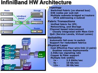
What is InfiniBand • Switched fabric communication link • 2.5 Gbit/s signaling • Primarily used in supercomputers • Specification maintained by the InfiniBand Trade Association • Protocol Stack • Physical Layer • Link Layer • Network Layer • Transport Layer
IP Cores Reusable hardware cores accelerate development E.g. DSP, communication controllers, cryptographers, memory, processors, Ethernet MAC Opencores.org
Problem/Need Currently have to use proprietary hardware interface (e.g. Mellanox) Can’t perform research on internals Need a open-source hardware implementation
Design Concept Hardware core in VHDL Compatible with InfiniBand specifications Implementation on an FPGA or in simulator
Operating Environment • Proprietary Environments • Xilinx ISE (Development Environment) • ModelSim (Simulator) • Virtex-5 Development Board
User Interface • No UI in conventional terms • VHDL Synthesizer • VHDL Simulator • FPGA pinout
Functional Requirements • FR01: The system shall provide InfiniBand compliant input/output signals. • FR02: The system shall be able to transmit and receive packets according to InfiniBand specifications. • FR03: The system shall be able to handle errors according to InfiniBand specifications.
Nonfunctional Requirements • NFR01: The system shall be written in VHDL. • NFR02: The system shall be distributed under an open source license. • NFR03: The system should use only standard VHDL libraries. • NFR04: The system should be compatible with open source VHDL simulators.
Market Research • InfiniBand Trade Association (Cisco, IBM, Intel, etc.) maintains specification • No open-source IP core competitors • Specification is freely available/open
Deliverables • CD containing: • Source Code (VHDL) • Compilation Instructions • User’s Manual • Submit to OpenCores.org
Resources • Team Members (Alex Burds, Tim Prince, Matt Wall, Ryan Schwarzkopf, Xiang Li) • Ryan Schwarzkopf (Communications Coordinator) • Matt Wall (Project Leader) • Jason Boyd (Lab Coordinator) • Dr. Morris Chang (Project Advisor) • Troy Benjegerdes (Client) • Lab with Virtex-5 board and compatible synthesizer (Coover 2041)
Schedule Overview • Implementation begins – 1/12/09 • Layers completed – 4/3/09 • Layers tested – 4/22/09 • System integration completed – 4/26/09 • Integration testing completed – 4/26/09 • System testing completed – 4/29/09 • Documentation completed – 5/4/09 • Bound Report completed – 5/4/09
Identified Risks • Complexity of system may prevent complete hardware implementation • Complete testing may require more time than is available • May need to obtain additional test equipment
System Overview • Two Layers • Link • Physical • Top-down design approach
Link Layer • Handles the sending and receiving of data across the links at the packet level • Provides addressing, flow control, and error detection • Virtual Lanes provide buffering • Link State Machine responds to changes in the link status
Components Link State Machine Packet Receiver Machine Data Packet Check Machine Link Packet Check Machine Flow Control Generator Virtual Lane Arbitration CRC Generators
Virtual Lanes • Buffer packets to and from Link Layer • Two VLs required, VL0 and VL15 • VL15 reserved for subnet management packets
Flow Control • Prevent buffer overflow • Send flow control packets periodically • Updates credit information from Virtual Lane • Stop transmitting if receiver doesn’t have enough credits
Packet Check Machines Data Packet Check Machine • Variable packet headers and payloads mean more robust error checking • Error checks performed by DPCM • VCRC and ICRC check • Link version check • Destination Local Identifier check • VL and VL15 checks • Buffer availability check • Verifies the length of the packet • Reports errors in correct precedence and discards packets with errors • Error free packets passed to Virtual Lane
Packet Check Machines Link Packet Check Machine • Only one type of packet (flow control packet) • Checks for errors within a link packet • Verifies Link Packet CRC • Flow control opcode is flagged • Verifies correct virtual lane is selected and supported • Verifies the length of the flow control packet (6 Bytes) • Reports errors in correct precedence and discards packets with errors • Error free packets passed to Virtual Lane
CRC Generators Two CRC Types • Variant • Entire Packet (Including Payload) • Changes between transmissions • Invariant • Data payload • Static
Physical Layer • Maintains physical link • Three main components • Link/Phy Layer • RocketIO Adapter • RocketIO Module
Link/Physical Layer Manages link training process Maintains link state once completed Inserts control sequences to allow clock synchronization
Link Training FSM Maintains link state Handles errors
RocketIO Adapter • Manages Xilinx RocketIO operation • Clock generation and recovery • 8b/10b Encoding • Converts Link/Phy control signals into the equivalent RocketIO signals
Simulation Testing • Simulate individual components to determine if they behave as expected • Integrate components in a layer to determine if they work together • Use ModelSim VHDL simulation
Integration Testing • Once individual layers are simulated, we will progressively integrate them together and physically test them • Phy/Phy testing • Connect the Physical layer programmed on a single board through loopback and ensure that a data stream can be transmitted
Integration Testing Contd. • Phy+Link/Phy+Link • Add the Link layer and determine if packets can be transmitted. • Also check for packet integrity and flow control behavior
Test Harness • Instance of the link and physical layers • PLB control interface • Programmable interconnects • Inject and extract data into and out of the data-path
Accomplishments Physical Layer compiles Physical Layer simulation Physical Layer physical testing Link Layer compiles Link Layer simulation Performed extended testing with a 5-10 Giga-sample oscilloscope
Challenges Debugging the serial loop back Switching from Vertex-II to Vertex-5 board Only having 1 Vertex-5 board VHDL intense project Lost a team member
Conclusion Have a springboard for further development Further verification and development is needed for a robust IP core
Lessons Learned Evaluate project complexity in greater detail Divide tasks into smaller parts Set stricter guidelines for tasks Obtain clearer end goal from client Define specific skill set required
Future Work Verification of layers against specifications in detail Potentially port to different transceivers Create an open hardware development platform Make more robust for usability