Chapter 12 Memory Organization
Chapter 12 Memory Organization. Dr. Bernard Chen Ph.D. University of Central Arkansas Spring 2009. Memory Hierarchy. The memory unit is an essential component in any digital computer since it is needed for storing programs and data


Chapter 12 Memory Organization
E N D
Presentation Transcript
Chapter 12 Memory Organization Dr. Bernard Chen Ph.D. University of Central Arkansas Spring 2009
Memory Hierarchy • The memory unit is an essential component in any digital computer since it is needed for storing programs and data • Not all accumulated information is needed by the CPU at the same time • Therefore, it is more economical to use low-cost storage devices to serve as a backup for storing the information that is not currently used by CPU
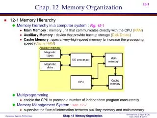
Memory Hierarchy • The memory unit that directly communicate with CPU is called the main memory • Devices that provide backup storage are called auxiliary memory • The memory hierarchy system consists of all storage devices employed in a computer system from the slow by high-capacity auxiliary memory to a relatively faster main memory, to an even smaller and faster cache memory
Memory Hierarchy • The main memory occupies a central position by being able to communicate directly with the CPU and with auxiliary memory devices through an I/O processor • A special very-high-speed memory called cache is used to increase the speed of processing by making current programs and data available to the CPU at a rapid rate
Memory Hierarchy • CPU logic is usually faster than main memory access time, with the result that processing speed is limited primarily by the speed of main memory • The cache is used for storing segments of programs currently being executed in the CPU and temporary data frequently needed in the present calculations • The typical access time ratio between cache and main memory is about 1to7 • Auxiliary memory access time is usually 1000 times that of main memory
Main Memory • Most of the main memory in a general purpose computer is made up of RAM integrated circuits chips, but a portion of the memory may be constructed with ROM chips • RAM– Random Access memory • In tegated RAM are available in two possible operating modes, Static and Dynamic • ROM– Read Only memory
Random-Access Memory (RAM) • Static RAM (SRAM) • Each cell stores bit with a six-transistor circuit. • Retains value indefinitely, as long as it is kept powered. • Relatively insensitive to disturbances such as electrical noise. • Faster and more expensive than DRAM. • Dynamic RAM (DRAM) • Each cell stores bit with a capacitor and transistor. • Value must be refreshed every 10-100 ms. • Sensitive to disturbances. • Slower and cheaper than SRAM.
SRAM vs DRAM Summary Tran. Access per bit time Persist? Sensitive? Cost Applications SRAM 6 1X Yes No 100x cache memories DRAM 1 10X No Yes 1X Main memories, frame buffers
ROM • ROM is used for storing programs that are PERMENTLY resident in the computer and for tables of constants that do not change in value once the production of the computer is completed • The ROM portion of main memory is needed for storing an initial program called bootstrap loader, witch is to start the computer software operating when power is turned off
Main Memory • A RAM chip is better suited for communication with the CPU if it has one or more control inputs that select the chip when needed • The Block diagram of a RAM chip is shown next slide, the capacity of the memory is 128 words of 8 bits (one byte) per word
Memory Address Map • Memory Address Map is a pictorial representation of assigned address space for each chip in the system • To demonstrate an example, assume that a computer system needs 512 bytes of RAM and 512 bytes of ROM • The RAM have 128 byte and need seven address lines, where the ROM have 512 bytes and need 9 address lines
Memory Address Map • The hexadecimal address assigns a range of hexadecimal equivalent address for each chip • Line 8 and 9 represent four distinct binary combination to specify which RAM we chose • When line 10 is 0, CPU selects a RAM. And when it’s 1, it selects the ROM
Auxiliary Memory • The average time required to reach a storage location in memory and obtain its contents is called the access time • The access time = seek time + transfer time • Seek time: required to position the read-write head to a location • Transfer time: required to transfer data to or from the device
Cache memory • If the active portions of the program and data are placed in a fast small memory, the average memory access time can be reduced, • Thus reducing the total execution time of the program • Such a fast small memory is referred to as cache memory • The cache is the fastest component in the memory hierarchy and approaches the speed of CPU component
Cache memory • When CPU needs to access memory, the cache is examined • If the word is found in the cache, it is read from the fast memory • If the word addressed by the CPU is not found in the cache, the main memory is accessed to read the word
Cache memory • The performance of cache memory is frequently measured in terms of a quantity called hit ratio • When the CPU refers to memory and finds the word in cache, it is said to produce a hit • Otherwise, it is a miss • Hit ratio = hit / (hit+miss)
Cache memory • The basic characteristic of cache memory is its fast access time, • Therefore, very little or no time must be wasted when searching the words in the cache • The transformation of data from main memory to cache memory is referred to as a mapping process, there are three types of mapping: • Associative mapping • Direct mapping • Set-associative mapping
Cache memory • To help understand the mapping procedure, we have the following example:
Associative mapping • The fastest and most flexible cache organization uses an associative memory • The associative memory stores both the address and data of the memory word • This permits any location in cache to store ant word from main memory • The address value of 15 bits is shown as a five-digit octal number and its corresponding 12-bitword is shown as a four-digit octal number
Associative mapping • A CPU address of 15 bits is places in the argument register and the associative memory us searched for a matching address • If the address is found, the corresponding 12-bits data is read and sent to the CPU • If not, the main memory is accessed for the word • If the cache is full, an address-data pair must be displaced to make room for a pair that is needed and not presently in the cache
Direct Mapping • Associative memory is expensive compared to RAM • In general case, there are 2^k words in cache memory and 2^n words in main memory (in our case, k=9, n=15) • The n bit memory address is divided into two fields: k-bits for the index and n-k bits for the tag field
Set-Associative Mapping • The disadvantage of direct mapping is that two words with the same index in their address but with different tag values cannot reside in cache memory at the same time • Set-Associative Mapping is an improvement over the direct-mapping in that each word of cache can store two or more word of memory under the same index address
Set-Associative Mapping • In the slide, each index address refers to two data words and their associated tags • Each tag requires six bits and each data word has 12 bits, so the word length is 2*(6+12) = 36 bits