5.1 Documentation Standards
This document outlines critical documentation standards necessary for designing and maintaining digital systems. It emphasizes the importance of comprehensive documentation, which should include circuit specifications, block diagrams, schematic diagrams, timing diagrams, structured logic device descriptions, and circuit descriptions. Each type of documentation serves a unique purpose, ensuring clarity and facilitating efficient communication about system functionality and architecture. Additionally, effective naming conventions and active levels for signals are discussed to enhance understanding in combinational logic design.

5.1 Documentation Standards
E N D
Presentation Transcript
Return Next 5.1Documentation Standards 1. Introduction • Most real combinational logic design problems are very large. By structured thinking, a complex circuit or system can be conceived by any human being, because such a circuit or system is built on a collection of subsystems, each of which has a simple description. • In combinational logic design, there are several straightforward structures — decoders, multiplexers, comparators. • Before launching into these combinational building blocks, we’ll discuss the documentation standards, circuit timing, etc.
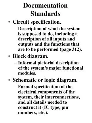
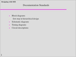
Return Back Next 5.1Documentation Standards 2. Documentation Standards Good documentation is essential for correct design and efficient maintenance of digital systems. A documentation package should generally contain at least the following six items: • A circuit specification describes exactly what the circuit or system is supposed to do, including a description of all inputs and outputs(“interfaces”) and the functions that are to be performed. • A block diagram is an informal pictorial description of the system’s major functional modules and their basic interconnections.
Return Back Next 5.1Documentation Standards • A schematic diagram is a formal specification of the electrical components of the system. • A timing diagram shows the values of various logic signals as a function of time. • A structured logic device description describes the internal function of a programmable logic device(PLD), FPGA, ASIC. • A circuit description is a narrative text document that, in conjunction with the other documentation, explains how the circuit works internally.
R/W IN ADDR 16-word32-bit BYTE EN RAM OUT RESET CONTROL LOAD RUN DISPLAY INBUS 32 32 32 32 32 2 32-BIT REGISTER 32 right direct left 32 MULTIPLEXER 4 TO 1 SEL A REGISTER B REGISTER 32 32 32 CARRY LOOKAHEAD ADDER 32-BIT REGISTER 474LS377 32 32 Block Diagrams
Return Back Next 5.1Documentation Standards • A block diagrams shows the inputs, outputs, functional modules, internal data paths, and important control signals of a system. In general, it should not be so detailed that it occupies more than one page, yet it must not be too vague. • Each block should be labeled with the function of the block, not the individual chips that comprise it. • The flow of control and data in a block diagram should be clearly indicated. • Bus is a collection of two or more related signal lines. In a block diagram, buses are drawn with a double or heavy line. A slash and a number may indicate how many individual signal lines are contained in a bus.
Return Back Next 5.1Documentation Standards 2) Gate Symbols (See P316-317) 3) Signal Names and Active Levels • In a real system, well-chosen signal names convey information to someone reading the logic diagram the same way that variable names in a software program do. e.g. GO, PAUSE, READY, ERROR, INBUS[31:0]) • Active level A signal is active high (low) if it performs the named action or denotes the named condition when it is HIGH or 1 (LOW or 0) (positive-logic).
1 1 15 15 Y0 Y0 A A 2 2 14 14 Y1 Y1 B B 3 3 13 13 Y2 Y2 C C 12 12 Y3 Y3 11 11 Y4 Y4 6 6 10 10 Y5 Y5 G1 G1 4 4 9 9 Y6 Y6 G2A G2A 5 5 7 7 Y7 Y7 G2B G2B 74LS138 74LS138 Return Back Next 5.1Documentation Standards 4) Active Levels for Pins (P319-320)
Return Back Next 5.1Documentation Standards 5) Bubble-to-Bubble Logic Design • The signal name on a device’s output should have the same active level as the device’s output pin — that is, active-low if the device symbol has an inversion bubble on the output pin, active-high if not. • If the active level of an input signal is the same as that of the input pin to which it is connected, then the logic function inside the symbolic outline is activated when the signal is asserted.
A SEL DATA ADATA_L A ASEL DATA B BSEL =ASEL·A+ASEL ·B B BDATA_L Return Back Next 5.1Documentation Standards • If the active level of an input signal is the opposite of that of the input pin to which it is connected, then the logic function inside the symbolic outline is activated when the signal is negated. This case should be avoided whenever possible because it forces us keep track mentally of a logical negation to understand the circuit. A 2-input multiplexer
Return Back 5.1Documentation Standards 6) Drawing Layout • Flat schematic structure (p324 Figure 5-14) • Hierachical schematic structure(p325 Figure 5-15) 7) Buses (p327 Figure 5-16) 8) Additional Schematic Information • (p328 Figure 5-17) • (p329 Figure 5-18)