Advanced Memory Configuration for High-Performance Computing Systems
190 likes | 286 Views
Explore the efficient 256-bit memory configuration with DDR SDRAM for improved data paths and performance in computing systems. Understand cache architecture, cache conflicts, and memory victim paths in multi-processor environments.

Advanced Memory Configuration for High-Performance Computing Systems
E N D
Presentation Transcript
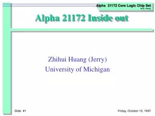
Alpha 21172 Inside out Zhihui Huang (Jerry) University of Michigan
Components • One 21172-CA chip • Control, I/O, address chip(CIA) • 388 pins, plastic ball grid array(PBGA) • Four 21172-BA • data switch chip (DSW) • 208 pins, plastic quad flat pack (PQFP)
Slowest part has the widest bus Data Paths • 64-bit data path between CIA and DSW • iod • 128-bit data path between 21164 and DSW • cpu_dat • 256-bit memory data path between DSW and memory • mem_dat
21164 DSW0 DSW1 DSW2 DSW3 DRAM 1 DRAM 2 DRAM 3 DRAM 4 DRAM 5 DRAM 6 DRAM 7 DRAM 8 64-bit IOD bus addr<39:4> 21172 RAS CAS control memadr<11:0> 64-bit PCI Bus 3-way Interface Vein Brain Heart
128 bit SIMM 1 SIMM 2 SIMM 3 SIMM 4 SIMM 5 SIMM 6 SIMM 7 SIMM 8 256-bit Memory The DRAM is contained in one bank of SIMMs,whether there are 4 SIMMs or 8 SIMMs. DRAM 1 DRAM 2 DRAM 3 DRAM 4 DRAM 5 DRAM 6 DRAM 7 DRAM 8 4 SIMMs fill a data bus of 128 bits 8 SIMMs fill a data bus of 256 bits Needs a jumper
DSW0 DSW1 DSW2 DSW3 128-bit 128-bit DRAM 1 DRAM 2 DRAM 3 DRAM 4 DRAM 5 DRAM 6 DRAM 7 DRAM 8 256-bit Memory block It is better to use the 256-bit configuration, or you pay the full price for DSWs and only use half of the resources. A 256-bit block is composed of bit slices across all the 8SIMMs The arrangement of the slices are interleaved within the 4 DSWs It may be clear now why it is a onebank schema with all the SIMMs have the same size. 15:0 79:64 31:16 95:80 47:32 102:96 63:48 127:102 As you just see, the 4 DSWs together provide the lower 128-bit memory bus. For the 256-bit configuration, DSWs also provide the upper part of the bus
In the PC164 ECC protected • A cache where the cache location for a given address is determined from the middleaddress • bits. If the cache line size is 2^n then the bottom n address bits correspond to an offset within a cache entry. • If the cache can hold 2^m entries then the next m address bits give the cache location. The remaining top • address bits are stored as a TAG along with the entry. • In this scheme, there is no choice of which block to flush on a cache miss since there is only one place for • any block to go. This simple scheme has the disadvantage that if the program alternately accesses different • addresses which map to the same cache location then it will suffer a cache miss on every access to these locations. • This kind of cache conflict is quite likely on a multi-processor. Bcache and Memory A cache architecture in which data is only written to main memory when it is forced out of the cache. Opposite of write-through. The Scache and Bcache block size is either 64-bytes or 32 bytes. The Scache and Bcache always have identical block sizes. All the Bcache and main memory FILLs or write transactions are of the selected block size. A cache line is allocated when the write memory data miss the cache • 3rd Level Cache for the 21164 • Attributes • optional, external,physical, synchronous SRAM • direct-mapped, write-back,write-allocate • 256-bit or 512-bit block • cache size of 1,2,4,8,16,32,64 Mbytes • support up to 512MB of memory • 1MBx36, 2MBx36,4MBx36,8MBx36,16MBx36
clk Frame# data data addr PCI features • Supports 64-bits PCI bus width • Supports 64-bit PCI addressing (DAC cycles) • Accept PCI fast back-to-back cycles • addr,data0,data1,data2,...,addr_again! • The Frame# is only deasserted for a cycle to allow the last to finish • Issues PCI fast back-to-back cycles in dense addrss space
CIA Transactions • 21164 memory read miss • 21164 memory read miss with victim • 21164 I/O read • 21164 I/O write • DMA read • DMA read(prefetch) • DMA write
Memory Victim Path 21164 BCache SYS MEM Read Miss Path IO Paths not shown Instruction Queue DMA 0 DMA 1 PCI Flush Flush PCI MEM IOD IOD MEM MEM SYS SYS DSW Data Paths
DSW Buffers • DMA Buffer Sets (0 and 1) • PCI buffer for PCI DMA write data • Memory buffer for memory data • Flush buffer for system bus data DMA 0 DMA 1 PCI Flush Flush PCI IOD IOD MEM MEM
DMA Writes Memory • Data arrives in the PCI Buffer • Memory Buffer loaded at the same time • Bcache line flushed and Flush buffer loaded • 3 sources merged and data back at memory As you just see, the DMA operation causes PCI buffer loaded from the IOD bus, the MEM buffer loaded from memory, and the flush buffer loaded from system bus at the same time Then the 3 sources are merged and written back to main memory DMA 0 21164 BCache Flush PCI IOD MEM
Memory 21164 BCache SYS MEM Read Miss Path Read data Data back to CPU 21164 Read Transaction • If hit in the Bcache, no memory access is required HIT !!
21172 CIA Read data Data back to CPU Command 21164 Read Miss • If not hit in the Bcache during a read, memory access is involved. command Memory 21164 BCache 21172 BA Miss!! SYS MEM Read Miss Path
Read Missed block and Write victim block are indivisible in the logic design 21172 CIA Write data Command Read Miss With Victim • Two scenarios • write data with different address tag into a valid cache line • read data with different address tag into a valid cache line Write allocate!! read allocate!! command Memory Victim Path 21164 BCache Merge data Miss!! SYS MEM Read Miss Path
All the circle parts compete for this resource Memory 21164 BCache Cause read miss Cause read miss with victim SYS MEM Read Miss Path Traffic Jam on MEM bus Don’t forget instruction fetch uses memory too Let’s think about this senario, during the PCI DMA transfer, there are READ and WRITE memory happening at the same time Victim Path IO Paths not shown Instruction Queue DMA 0 DMA 1 PCI Flush Flush PCI MEM IOD IOD MEM MEM SYS SYS
33 MHz PCI has the same speed with DRAM !! Can we really do this ?? 60 ns DRAM 256-bit bus 33MHz PCI 64-bit bus How Fast can DMA be? • 2 fetches and 2 writes to memory/DMA • 64 bytes/240 ns = 266 Mbytes/s • 8 bytes /30 ns = 266 Mbytes/s Overhead, retrys, read lines, read line with victim, instruction fetch all share the same bandwidth!! It turns out for the worst case, 17MBytes/s is achieved just above bottom line DMA 0 DMA 1 PCI Flush Flush IOD IOD MEM MEM SYS SYS
Performance of the MB2PCI • Worst case • 29.9MBytes/s • 25.5MBytes/s • 17.5MBytes/s • Best case • 95MBytes/s • 80MBytes/s • 72MBytes/s - No intervenence - read line, instruction fetch - read line, read line with victim, instruction fetch
Conclusion • If we want to improve • use 256-bit cache block instead of 512-bit • Is there a next version 21172 chip surport 512-bit memory bus? • Is there DRAM chips faster then 60ns • can we afford 64M Bcache(SRAM)? There is a trade off here, by using smaller block, the 21164 will generate more cache miss cycles and may slow down. On the other hand, for the DMA transfer, when only 128-bit data is transferred, no more 512-bit memory read overhead. There is only 256-bit read now. Thus improve the worst case performance.