NBTI(Negative Bias Temperature Instability)
671 likes | 1.96k Views
NBTI(Negative Bias Temperature Instability). MiDAS Lab. C.N.U 2003. 10. 06 Park Young Ho http://midaslab.cnu.ac.kr. Contents. 1. Introduction 2. Physical Model of NBTI Mechanism 3. Experiments 4. Device Degradation due to NBTI 5. Origin of NBTI

NBTI(Negative Bias Temperature Instability)
E N D
Presentation Transcript
NBTI(Negative Bias Temperature Instability) MiDAS Lab. C.N.U 2003. 10. 06 Park Young Ho http://midaslab.cnu.ac.kr
Contents • 1. Introduction • 2. Physical Model of NBTI Mechanism • 3. Experiments • 4. Device Degradation due to NBTI • 5. Origin of NBTI • 6. Effect of Nitrogen Incorporation into Gate Oxide • 7. The Way to Reduce/Strengthen the Weak Silicon Bonds • 8. Process Dependence of NBTI • 9. Influence of Nitrogen Proximity from the Interface • 10. Conclusions
1. Introduction • NBTI(Negative Bias Temperature Instability) has become increasingly serious as the device dimensions are continually scaled down. • NBTI degradation -> Vth Shift of pMOSFETs -> begin to limit the device lifetime • A good understanding of the physical mechanism responsible for NBTI is basic to the minimization of this degradation mode.
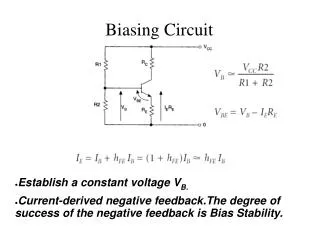
2. Physical Model of NBTI Mechanism ≡Si-H : hydrogenated trivalent silicon A : neutral water-related species at the interface P+ : hole at the silicon surface ≡Si* : neutral trivalent silicon(i.e.,interface state) H+ : positively charged interstitial hydrogen ion
5. Origin of NBTI(2) • Diffusion of hydrogen related species play a major role for NBTI • The hydrogen terminated silicon bond is the precursor for fixed charges and interface states • weak silicon bonds at the interface • Nitridation
6. Effect of nitrogen incorporation into gate oxide(1) • Nitridation of the gate oxide has a great influence on NBTI and it enhances the Vth shift • Nitridation degrades the device lifetime
6. Effect of nitrogen incorporation into gate oxide(2) • Higher nitridation decreases the allowable maximum operation temperature
6. Effect of nitrogen incorporation into gate oxide(3) • Nitridation does not increase initial leakage current • But, after NBTI stress, a large increase around the VFB was observed for nitrided oxide
6. Effect of nitrogen incorporation into gate oxide(4) • The concentration of nitrogen in the gate oxide has to beoptimized in terms of the reliability reduction due to NBTI, for highly reliable MOS devices.
7. The way to reduce/strengthen the weak silicon bonds (1) • (1) Introduce an appropriate amount of fluorine by ion implantation into the gate oxide
7. The way to reduce/strengthen the weak silicon bonds (2) • (2) The use of deuteriumPMA(Post Metal Anneal) - passivate the dangling bonds - The bonds to deuterium are more difficult to break than bonds to hydrogen
8. Process dependence of NBTI(1) • NISS(Nitrogen Implanted Silicon Substrate) • N2O(N2O-nitrided oxide) • RTNO(Rapid Thermal Nitrided Oxide) • RPNO(Remote Plasma Nitrided Oxide)
8. Process dependence of NBTI(2) • RPNO(Remote Plasma Nitrided Oxide) - (1) Oxynitride formed can incorporate more nitrogen to achieve higher dielectric constant, effectively reduce leakage current, and suppress boron peneration. - (2) extends the reliability scaling limit of SiO2-based gate dielectrics - (3) most resistant to the NBTI stress
8. Process dependence of NBTI(4) • N2 I/I + RPNO : nitrogen ion implantation prior to RPNO • RPNO(L) : RPNO with lower nitrogen concentration • RPNO(H) : RPNO with higher nitrogen concentration
8. Process dependence of NBTI(5) • Among the various gate dielectrics under consideration, RPNO is most resistant to NBTI stress. • However, the nitrogen concentration introduced in the RPNO process needs to be optimized because too much nitrogen content may weaken trivalent silicon bond energy due to excessive stress and therefore enhance NBTI degradation.
9. Influence of Nitrogen Proximity from the interface(1) • NBTI lifetime increases significantly by removing the nitrogenaway from the Si/SiO2 interface • DPNO(Decoupled Plasma Nitrided Oxides) • RPNO(Remote Plasma Nitrided Oxides) more resistant to the nitrogen-enhanced NBTI effect as compared to RTNO(Rapid Thermal Nitrided Oxides)
9. Influence of Nitrogen Proximity from the interface(2) • Plasma nitridation yields a nitrogen-rich layer at the top oxide surface, • while thermal nitridation generally results in a sharp nitrogen distribution • located at the Si/SiO2 interface.
9. Influence of Nitrogen Proximity from the interface(3) • PNRO(Post Nitridation Re-Oxidation) following RTNO process would • displace the nitrogen peak away from the Si/SiO2 interface
10. Conclusions • The density of hydrogen terminated silicon bond at the interface needs to be minimized • The concentration of nitrogen in the gate oxide has to be optimized • The impact of nitrogen on NBTI diminishes as the nitrogen is removed away from the Si/SiO2 interface