RCU Status
190 likes | 356 Views
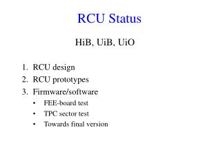
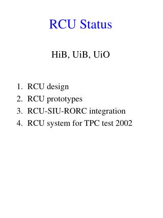
RCU Status. HiB, UiB, UiO. RCU hardware Firmware/Software Test setups. Readout Contoller Unit. 1. RCU hardware. Prototype I 3 commercial PLDA PCI boards (two at CERN) FEC test (ALTRO + FEE bus) SIU integration Qtr 3, 2001 – Qtr 3, 2002 Prototype II Custom design

RCU Status
E N D
Presentation Transcript
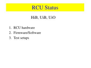
RCU Status HiB, UiB, UiO • RCU hardware • Firmware/Software • Test setups
1. RCU hardware • Prototype I • 3 commercial PLDA PCI boards (two at CERN) • FEC test (ALTRO + FEE bus) • SIU integration • Qtr 3, 2001 – Qtr 3, 2002 • Prototype II • Custom design • All functional blocks • PCB: pre-prototype: June 2002, full prototype: September 2002 • Implementation of basic functionality (FEE-board-> SIU): Qtr 4, 2002 • Implementation of essential functionality: Qtr 2, 2003 • Prototype III • Minimal implementation • Form factor adapted to sector geometry • SRAM FPGA -> masked version or Antifuse FPGA (if needed) • RCU production • Qtr 2, 2003
DCS Profi-bus FEE-bus DCS Ether-net TTC rx FEE-bus FEE SC FPGA PCI core PCI bus internal SRAM SIU SIU-CMC interface FLASH EEPROM memory RCU prototype II • Implementation of essential functionality • Custom design • All functional blocks
RCU prototype II • Costs (August 2002) • dominated by FPGA + SRAM • FPGA EP20K400EFC672 • speed grade 3: 350 EUR • speed grade 1: 700 EUR • SRAM (32bit + 64bit) • 0 + 2 MByte: 40 EUR • 8 + 4 Mbyte: 240 EUR • all other components • approx. 200 EUR • total component cost • fully loaded: 1140 EUR • minimal: 590 EUR
RCU prototype II • Motherboard • FPGA • memory data buffer • memory work space • ethernet • PCI interface • CMC connectors • Mezzanine card I • SIU • Mezzanine card II • FEE bus A and B • TTCrx • Profibus interface
RCU prototype II - motherboard 107 mm x 314 mm
RCU prototype II – status (1) • Status motherboard (in collab. with HD) • 3 working prototypes • Basic functionality • ALTERA PCI core • external 32 bit and 64 bit memory • NIOS core • Ethernet • RCU functionality • PLDA PCI core • FEB / SIU programs • 8 more prototypes in production
RCU prototype II - status (2) • Status RCU mezzanine board • 2 boards fully loaded • 2 x FEC-bus • TTCrx • Profibus • 6 boards with minimal configuration • FEC-bus • Layout finished, PCB production and mounting of components at UiO (David Wormald) in September
2. RCU firmware design – control flow TTCrx SIU controller FEE bus controller • State machines DDL command decoder FEE SC RCU resource & priority manager Huffman encoder DCS low level Watchdog 2 Watchdog 1: health agent Debugger DCS high level PCI core
Firmware/software – status and plans • FEC-bus controller • Jørgen Lien and ALTRO crew • SIU controller • Jørgen and Csaba Soos • DCS • Jon Wikne (UiO) and FH Worms • TTCrx Interface • Sten Solli (UiO) • SEU watchdogs • UiB
FEC/SIU controller – current RCU setup • Based on the PLDA commercial PCI-board • One PLDA-RCU reads out channel by channel up to 13 FECs • Data is stored in internal memory and transferred via PCI to the PC memory. This is done on a channel by channel basis. • Linux application (mini-DAQ, API, device driver) merges the data from each channel into one subevent.
RCU-FEE integration: ReadOut of ALTROs/FECs via PCI using PLDA prototype done (channel by channel) Configuration of ALTROs via PCI using the FE-Bus/ALTRO protocol done RCU-DDL integration: Transfer of data from PLDA-RCU ext. Memory to DDL (current SIU mezzanine) done Writing of status reg. on PLDA-RCU from DDL(SIU mezzanine) done Writing blocks of data from DDL (SIU mezzanine) to PLDA-RCU memory (int. and ext.) done Firmware status
Migration to prototype II – next steps • Transfer of current design to Prototype II (done). • Testing of data transfer from Prototype II external memory to new SIU card. • Building larger fragments (up to full subevent) in RCU external memory (consisting of data from all active channels on all ALTROs/FECs connected to the RCU front end branches) – optimize performance/latency vs memory usage. • Improve PCI readout speed by DMA engine • Merging the Front End and DDL/SIU designs to send data via the new SIU to the RORC/DAQ.
DCS • Backend interface to DCS • OPC server • Fieldbus • Profibus • Ethernet • Frontend interface • Profibus slave ASIC + SM • Ethernet chip + NIOS core
PROFIBUS • Profichip VPC3+B Evaluation Kit including Slave board, Software (incl. source code C) • 5 pcs programmable PROFIBUS-DP Slave Controller ASICs • Hilscher Master-Card CIF50-PB (PCI-interface, incl. software) • 3 pcs Profichip EasyConn PB diagnostic plugs with P/D sockets • 10 m profichip PROFIBUS cable type A (EN 50170) • OPC server licence
TTCrx interface • Firmware development • Model the TTCrx ASIC with VHDL • Emulate the TTC system stimulating the TTCrx model • Code the communication between the RCU FPGA and the TTCrx • Trigger system test • Need “TPC local trigger crate” • Where? CERN or Oslo/Bergen? • Who?
FEE-boards RCU system for TPC test: end 2002/2003 RCU prototype II Trigger FEE-bus LINUX RH7.2 FEE configurator PCI-tools RCU-API device driver SIU FPGA interface FEE-bus controller SIU controller Manager PCI core SIU SRAM FLASH ext. SRAM PCI bus DDL RORC DIU LINUX RH7.2 DATE 4 DDL/PCI-tools HLT-RORC-API device driver FPGA interface PCI core DIU PCI bus