Download
1 / 42
830 likes | 1.84k Views
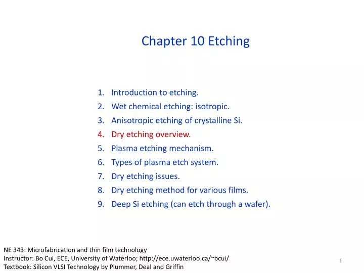
Chapter 10 Etching. Introduction to etching. Wet chemical etching: isotropic. Anisotropic etching of crystalline Si. Dry etching overview. Plasma etching mechanism. Types of plasma etch system. Dry etching issues. Dry etching method for various films.

E N D
Chapter 10 Etching • Introduction to etching. • Wet chemical etching: isotropic. • Anisotropic etching of crystalline Si. • Dry etching overview. • Plasma etching mechanism. • Types of plasma etch system. • Dry etching issues. • Dry etching method for various films. • Deep Si etching (can etch through a wafer). NE 343: Microfabrication and thin film technology Instructor: Bo Cui, ECE, University of Waterloo; http://ece.uwaterloo.ca/~bcui/ Textbook: Silicon VLSI Technology by Plummer, Deal and Griffin
Why dry etching? • Dry etching advantages • Eliminates handling of dangerous acids and solvents • Uses small amounts of chemicals • Isotropic or anisotropic/vertical etch profiles • Directional etching without using the crystal orientation of Si • Faithful pattern transfer into underlying layers (little feature size loss) • High resolution and cleanliness • Less undercutting • Better process control • Dry etching disadvantages: • Some gases are quite toxic and corrosive. • Re-deposition of non-volatile compound on wafers. • Expensive equipment ($200-500K for R&D, few million for industrial tools ). • Types of dry etching: • Non-plasma based - uses spontaneous reaction of appropriate reactive gas mixture. • Plasma based - uses radio frequency (RF) power to drive chemical reaction.
Non-plasma based dry etching This is very rare. For example, Although there is a large gain in free energy, the large activation energy does not allow low temperature processes - reaction is only effective above 800°C. In order to succeed with “gas” etching, one has to go out of equilibrium. The solution is plasma etching. One exception is room temperature XeF2 etching of Si. (same for BrF3 & ClF3) 4Si(s) + 2Cl2 (g) ---> 4SiCl4 (g) + 130 kcal/mole Xenon di-fluoride (XeF2) etching of Si: 2XeF2 + Si 2Xe (g) + SiF4 (g) • XeF2 is a white powder, with vapor pressure 3.8 Torr at 25oC. • Isotropic etching, non-polish etching (rough) • High selectivity for Al, SiO2, Si3N4, photoresist, and PSG (phospho-silicate glass). • Typical etch rate 1μm/min • Heat is generated during exothermic reaction • XeF2 reacts with water (or vapor) to form HF Gas phase etching, no stiction between freed structure and substrate (no liquid involved like KOH etch, so no need of drying that collapses pattern due to capillary force). Popular for MEMS application. MEMS: micro electro mechanical systems
Plasma-based etching • Directional etching due to presence of ionic species in plasma and (self-) biased electric field. (The self-bias electric field is not applied externally, but is created spontaneously in RF plasma) • Two components exist in plasma • Ionic species result in directional etching. • Chemical reactive species result in high etch selectivity. • Control of the ratio of ionic/reactive components in plasma can modulate the dry etching rate and etching profile. Plasma Neutrals (etchant gas) Ions Free radicals Gaseous products react adsorb surface
RF plasma chemistry RF plasma is more widely used for dry etching than DC plasma – is there DC plasma dry etching? CF4 plasma Figure 10-9
Loss mechanisms • As seen in previous slide, in a plasma, unstable particles are continuously generated. • The concentrations of ions, radicals, active atoms, & electrons increase until their loss rate is equal to the generation rate, forming a steady-state plasma. • Recombination of ions and electrons: they attract each other and are annihilated. • Drift, diffusion to walls: electrons are lost at conductive surfaces, chamber walls or electrodes. Ions are lost (converted to neutral particles) by contact with conductive surfaces, especially positive electrode. • Recombination of radicals: e.g. 2O O2. • Chemical reaction (what we want): e.g. 4F + Si SiF4 (fluorine radical combines with silicon wafer to produce silicon tetra-fluoride gas. This is a typical dry etching process.) Plasma TV In equilibrium, degree of ionization typically 10-3 - 10-6, very low, meaning majority gas not ionized. (plasma density = number of ions/cm3 typically 109 – 1013/cm3.) In a plasma TV, the recombination of ion-electron or radical, or de-excitation of atom or molecule, generates the colorful light we see.
Chapter 10 Etching • Introduction to etching. • Wet chemical etching: isotropic. • Anisotropic etching of crystalline Si. • Dry etching overview. • Plasma etching mechanism. • Types of plasma etch system. • Dry etching issues. • Dry etching method for various films. • Deep Si etching (can etch through a wafer). NE 343: Microfabrication and Thin Film Technology Instructor: Bo Cui, ECE, University of Waterloo, bcui@uwaterloo.ca Textbook: Silicon VLSI Technology by Plummer, Deal, Griffin
Plasma etching mechanism overview • In a plasma, reactive neutral chemical species (free radicals, e.g. F atoms or molecular species CF3) are mainly responsible for the chemical reaction due to their much greater numbers compared to ions (e.g. CF3+ is also reactive, but with low concentration in a plasma. But Ar+ is not reactive, and etches/sputters much slower than chemical etching, even when ion energy is high -- generally chemical etching is much faster than physical). • Those free radicals and molecules also serve as primary deposition species in PECVD. • Those free radicals are more abundant than ions because: 1) they are generated at lower threshold energy (e.g. < 8eV; in comparison, Ar is ionized at 15.7eV); and 2) they (uncharged radicals) have longer lifetime in the plasma. • The neutral radicals arrive at cathode surface by diffusion (thus non-directional). • Charged ions are accelerated to the cathode due to self-bias. • (Unless with very high energy of >100eV as in ion beam/sputter etching), ion itself doesn’t contribute significantly to the chemical reaction mostly due to its very low concentration, but ion bombardment can greatly enhance the chemical reaction in ion-enhanced etching. Figure 10-10
Chemical etch: highly selective, but isotropic • Due to their incomplete bonding (incomplete outer shells), free radicals (neutral, e.g. CF3 and F from CF4 plasma) are highly reactive chemical species. • Free radicals react with film to be etched and form volatile by-products. • Pure chemical etch is isotropic or nearly isotropic, and the etching profile depends on arrival angle and sticking coefficients of free radicals. • Free radicals (un-charged) in plasma systems have isotropic arrival angles. • The sticking coefficient S is very low, typically only S0.01 (i.e. most free radicals adsorb then just bounce back without reaction). • This leads to isotropic character of etch, as free radicals can etch area beneath the mask due to bouncing, as seen in the figure. The resulted profile has large undercut. Adsorption rate onto surface
Sticking coefficient S Most adsorbed species just left the adsorption site without doing anything, so S<<1. Figure 10-11 “Reaction”, here momentum transfer by physical bombardment, takes place at every shot, usually sputter off a few atoms, so S1.
Si etching with F radicals Isotropic etching
Etch byproducts should have low boiling point Low boiling point means very volatile, so it can be pumped away. This is not necessary for physical etching/sputtering, where etch product is sputtered off that ideally doesn’t fall on the other part of the wafer (re-deposition). Boiling points of typical etch products
Physical etch component in a plasma etch system (much less important than chemical etch) • Ionic species are accelerated toward each electrode by built-in self-bias. • The ionic species such as Cl2+, CF4+, CF3+ (or Ar+ in a purely physical sputter etch) strike wafer surface and remove the material to be etched. • Directional, non-selective - similar sputter yield for different materials. (But CF3+ can also etch Si chemically, then with high selectivity) • It may result in significant re-deposition. Ar plasma • Pure physical etch: sputter etching system • Self-bias few 100V, but low ion energy (order 10V) due to collision energy loss. • Thus very low milling rate in a sputter system, often for surface cleaning only. • Here is the case for sputter etching system with gas pressure order 10mTorr. • For a dedicated ion milling system (no plasma, see later slides), the pressure is 10-4Torr or even lower (cannot sustain a plasma), leading to large mean free path, high ion energy and high milling rate.
Ion enhanced etching (IEE): chemical etch assisted by physical bombardment • IEE is an anisotropic (due to directional ion bombardment) and highly selective (due to chemical reaction) etching process. • Reactive ion etch (RIE) is the most popular form of IEE. • Ion bombardment can enhance one of the following steps during chemical etch: surface adsorption, etching reaction (by physically damaging/weakening the chemical bond of the material to be etched), by-product (inhibitor layer) removal, and removal of un-reacted etchants. Inhibitor layer: e.g. fluorocarbon polymer formed from CHF3 during etching of SiO2. When removal rate << deposition rate, net deposition will occur, then the process becomes similar to PECVD!! Indeed, the RIE and PECVD are pretty similar tools, except PECVD is typically heated. Chemical etch enhanced by ion bombardment Inhibitor removed by ion bombardment Figure 10-13
IEE: first proof of etching mechanism Gas phase etch, with or without the aid of Ar ion beam. NO plasma. Very slow etch when pure chemical or physical etch alone The ion enhancement could be due to the damage/weakening of silicon lattice by ion bombardment, which makes the etching by XeF2 easier. The resulted profile will be anisotropic since the horizontal surfaces are much more bombarded than vertical ones. This is one example of CAIBE (chemically assisted ion beam etching), see later slides
Ion enhanced etching is highly anisotropic • Sidewall reactions can lead to an isotropic etch component. • To prevent sidewall etching, one can build up a passivation (inhibitor – inhibit chemical reaction) layer that protects it. • Then there is a competition between passivating and etching reaction. • For the feature base/horizontal surfaces, etch rates tend to be temperature independent because of ion energy input (i.e. inhibitor sputtered away by ions). • On sidewall, substrate temperature can play an important role as sidewall passivation depends on the volatility of the inhibitor that is controlled by temperature (cryo-etcher at below -100oC is available recently, then the sidewall passivation layer is not volatile). • Even without sidewall passivation, lower temperature still increases anisotropy since chemical attack of sidewall is suppressed at low temperature. (Attack of horizontal surfaces are assisted by ion bombardment)
Example: etching profile of Si or SiO2 High inhibitor deposition rate Low inhibitor deposition rate Teflon • Fluoropolymer (like Teflon) in CHF3 or CF4+H2 RIE of Si or SiO2 is the inhibitor. • If Ar gas is added, inhibitor is mainly removed by ion bombardment. So less attack of inhibitor on sidewall. • If O2 gas is added, inhibitor on sidewall is removed at faster rate than Ar ion, but the etch of inhibitor at horizontal surface is even faster. • Yet at very low temperature, inhibitor SiOxFy (not act as inhibitor at higher temperature when it is volatile) forms when O2 is added, which is the mechanism for fast anisotropic etching of Si using cryo-etcher. (deep Si etcher, popular for MEMS – micro electro mechanical systems) Figure 10-14
Anisotropy due to ion bombardment: summary • Due to its extremely low density, ions don’t contribute much to etching; neutral radicals do. • So even with directional ion bombardment, the overall etching can still be pretty isotropic. • For instance, SF6 etch of Si is very isotropic with large undercut like wet etch. • To achieve anisotropy, there are two mechanisms: • Energy-driven anisotropy: bombardment by ion disrupts an un-reactive substrate and causes damages such as dangling bonds and dislocations, resulting in a substrate more reactive towards etchant species (electron or photon can also induce surface activation). • Inhibitor-driven anisotropy: ion bombardment removes the inhibitor layer from horizontal surface (sidewall remain passivated), and reaction with neutrals proceed on these un-passivated surfaces only. • One may think that ions won’t help much due to its much lower density than radicals. But ion has sticking coefficient S1 (every ion bombardment counts), whereas radicals S0.01 (most radicals hit the surface and left without doing anything). Inhibitor-driven anisotropy Energy-driven anisotropy
Chapter 10 Etching • Introduction to etching. • Wet chemical etching: isotropic. • Anisotropic etching of crystalline Si. • Dry etching overview. • Plasma etching mechanism. • Types of plasma etch system. • Dry etching issues. • Dry etching method for various films. • Deep Si etching (can etch through a wafer). NE 343: Microfabrication and Thin Film Technology Instructor: Bo Cui, ECE, University of Waterloo, bcui@uwaterloo.ca Textbook: Silicon VLSI Technology by Plummer, Deal, Griffin
Plasma etching in barrel etchers • Barrel etcher: • Chemical etching only, isotropic and selective like pure wet etch. • Use plasma shield to keep ion bombardment from wafers, thus very little damage. • Poor uniformity edge to center. • Used in non-critical steps such as photoresist removal by O2 plasma (Barrel “asher” Polymer + O CO2 + H2O). Quartz tube Figure 10-15
Downstream etchers • Plasma is formed in a cavity which is separated from the etching chamber. • Wafers are shielded from bombardment. • Only neutral free radicals reach wafers. • Etching is completely chemical and isotropic. • High selectivity achievable - Si:SiO2 = 50:1 • Plasma may be generated by RF (13.56MHz) or by microwave (2.45GHz).
Plasma etching in parallel plate systems – plasma mode Parallel plate = capacitively coupled plasma (CCP) You will see later on ICP : inductively coupled plasma • Similar to PECVD except that etch gas is used instead of precursor gas. • Equal or larger (grounded to chamber) wafer electrode (which defines “plasma mode”) gives weaker ion bombardment of wafers (smaller DC voltage drop near larger electrode). • The etch is more uniform than barrel, but typically etches only one or a few wafers (cassette for barrel etcher) at a time. • Both chemical and physical etch occur (wafer “in contact” with plasma), though the later is weak, particularly at higher pressure when DC voltage drop near wafer is smaller. • Etching is fairly isotropic and selective due to the strong chemical component. Very often, plasma mode etching is considered as just a kind of reactive ion etching (RIE), but done at higher pressure. Of course, both plasma mode etching and RIE is plasma etching. Figure 10-7
Parallel plate etchers (regular RIE, low density plasma) • Absolutely the most important form of dry etching, though recently ICP (see later slides) is becoming more and more popular. • Compared to plasma mode: smaller wafer electrode (counter electrode grounded to chamber wall), lower pressure (<100mTorr), more physical bombardment (voltage drop many 100V). • Ion enhanced etching mechanism, (usually) directional/anisotropic and selective. RIE using parallel plate setup is low density plasma system (ions 108 – 1010/cm3), thus low etch rate. Here low (ion) density plasma also implies low density of free radicals. Thus low etching rate. VERY roughly, one can say that plasma consists of order 1% radicals (reactive neutral species) and 0.01% ions.
Reactive ion etch (RIE) Schematic RIE process Etching mask • Due to its simultaneous anisotropy and selectivity, RIE is intensively used. • Works for most semiconductors and dielectrics. • OK for few metals that form volatile etch products: Al (form AlCl3), Cu (CuCl2) (not really), Ti (TiF4, TiCl4), W (WF6), Cr (CrO2Cl2). a) Ion sputtering, b) reactive ion etching, c) radical formation (?), d) radical etching (most important) In RIE, ion energy is low (several 10s eV, << voltage drop near wafer surface, due to collision energy loss), and its number density is very low, thus negligible etching by ion bombardment. The name reactive “ion” etching is very misleading since ions don’t contribute directly to etching – it just “helps” chemical etching.
Ion energy vs. pressure for a plasma • Lower pressure (<10mTorr) increases mean free path as well as voltage drop near wafer electrode, both of which leads to more energetic and directional ion bombardment, thus more anisotropic, but less selective and slower etching rate due to low ion/free radicals density. • High pressure (>100mTorr), short mean free path, low voltage drop, isotropic chemical etching. • Thus it is desirable to have a low pressure plasma with high ion density. Plasma mode: >100mTorr RIE mode: 10-100mTorr Sputter etching: pressure as low as possible, as long as plasma can be sustained, but still very slow etching rate. RIE with tilted wafer, will etch vertically or not?
Etching in high density plasma (HDP) systems • Ion flux and ion bombarding energy can be independently controlled. For regular RIE, they are tightly coupled (e.g. higher power increases both). • High plasma (ion) density (> 1011) enhances etch rate. • Since ionization is much more efficient, can operate at lower pressure, which leads to less ion collision, so more directional/anisotropic, thus enhances profile control. • As ion energy is independently controlled, it can be kept low if desirable. • Then the extent and amount of damage will be reduced, without sacrificing etching rate that is still high for high density plasma. • Currently HDP represents an optimum compromise in high etch rates, good selectivity, good directionality, while low ion energy and damage (??). • (What I think) For sidewall profile control and selectivity, hard to say which one (regular RIE vs. HDP) is better. But if wanted one can always turn off the HDP power, then the machine operates like a regular RIE. • The bottom line: for deep etching (>>1m) that needs very high etching rate, HDP is the only choice.
Electron cyclotron resonance (ECR) and inductively coupled plasma (ICP) ECR was introduced in 1985. ICP was introduced much later (1991- 1995). Dual plasma source: Top one (ECR or ICP RF power) generates HDP, determines ion density/current. Bottom one (CCP RF power) generates bias voltage like regular RIE, determines ion energy. Typical parameters for HDP and conventional plasma etcher ions/cm3 should be lower CCP: capacitively coupled plasma, parallel plate, used for conventional regular RIE.
ECR and ICP Electron cyclotron resonance plasma (less common nowadays) Inductively coupled plasma (ICP) (four systems at Waterloo) ICP RF power (for dense plasma) plasma RF bias power (similar to RIE, parallel plate) • High magnetic field in the coil, so electrons move in circles with long path, leading to higher collision and ionization probability, and much less electron loss to chamber wall and the bottom plate where sit the wafer. Moreover, • For ICP, AC magnetic field induces circular electrical field, which accelerates electrons. • For ECR, DC magnetic field, electron cyclotron =qB/m; electrons accelerated if this frequency matches the microwave frequency.
Microwave source 2.45 MHz Quartz window Wave guide Plasma chamber Diffuser Cyclotron magnet Wafer Additional magnet 13.56 MHz Electrostatic chuck Vacuum system Schematic of ECR etcher
Schematic of ICP etcher Inductive coil RF generator Dielectric window Plasma chamber Electromagnet Biased wafer chuck Bias RF generator As you see, there is practically no top plate as in parallel plate regular RIE. The wafer sees the ICP power – the two power sources are not physically separated. Otherwise, even though the plasma density in the upper part is high, it will get lost due to re-combination and de-excitation when it travels through the bottom part.
Electromagnet (1 of 4) Wafer Biased wafer chuck 13.56 MHz Magnetically enhanced reactive ion etch (MERIE) Like regular parallel plate RIE, but magnetic field forces electron to go circles, increasing collision with gas molecules and decreasing loss to chamber walls or top/bottom plates. However, now that electrons don’t loss to bottom plate, no or little bias voltage – need to apply an external bias to accelerate ions. I haven’t seen any MERIE, so it is not popular. On the contrary, magnetron sputtering is very popular. This is probably because there are many ways to increase etching rate; but sputter without magnetron is always very slow: few nm/min, vs. 10s to 100s nm/min RIE etching rate.
Sputter etching and ion milling • Sputter etching: (etch inside plasma) • The etch mechanism is purely physical and ion energies are greater than 500 eV. • Very similar in principle to sputter deposition, but now the target becomes substrate to etch. • Poor selectivity (2:1 or 1:1), very anisotropic. • Sputtering rate depends on sputter yields which can be a function of incident angle. • Problems include faceting (sputter yield is a function of incident angle), trenching, re-deposition, charging and ion path distortion, radiation damage. • Not popular, etches too slow, though reactive gas (CF4, CCl4, O2) can be added to slightly improve selectivity and etching rate. Figure 10-8 Problems associated with sputter etching (or any etching that has a high degree of physical/ionic etching): a) trenching at bottom of sidewalls; b) redeposition of photoresist and other materials; c) charging and ion path distortion.
Ion milling or ion beam etching (IBE) Used to call ion milling, seems now more called as ion beam etching. • Physical milling when using heavy inert gases (Ar). • Plasma is used to generate ion beam (Ar+), which is extracted and accelerated to etch the sample. (i.e. sample outside of plasma) • Thus the ion density (determined by plasma source) and ion energy (determined by DC acceleration voltage – bias by applied DC voltage, not by RF bias as in high density plasma etching system), can be controlled independently. • Low pressure 10-4Torr (>1 order lower than RIE), so large mean free path and less energy loss due to collision. (such low pressure cannot sustain a plasma, so ion milling is not plasma etching) • High acceleration voltage (>1kV), leading to mill rate 10-30nm/min. • Despite the high voltage and low pressure, such a rate is still < typical RIE rate where chemical etching dominates. • Used whenever RIE is not possible (due to the lack of volatile species formation). Usually employed to etch Cu, Ni, Au, superconducting materials containing metals…
Ion beam etching system: triode configuration Electron beam is first generated by hot filament. Ions are generated by electron bombardment, then accelerated to bombard the substrate. RF plasma ion beam source (here reactive gas added, so it is actually a CAIBE, see next slide) DC plasma ion beam source Electrons sprayed to sample to neutralize ions. Tilted sample to greatly increase milling rate. But then shadowing may become a problem when milling high aspect ratio structures.
Chemically assisted ion beam etching system • Adding reactive gases (CF4, CCl4, O2, Cl2) to increase etching rate and selectivity. • Usually physical etching still dominates, no need of volatile etch product. • But for some special situations, like gas phase (no plasma) XeF2 etching of Si assisted by ion bombardment, chemical etching dominates with very high etching rate. But there the etch product SiF4 is volatile. • Here it is chemically assisted physical etching, different from RIE that is a kind of physically assisted chemical etching. • CAIBE: chemically assisted ion beam etching, inert Ar ion, neutral reactive gas is introduced into lower chamber, so not ionized, though some may be ionized due to backflow into plasma region or bombardment by Arion. • RIBE: reactive IBE, reactive gases are introduced into plasma region together with Ar gas, so they are ionized. RIEB is virtually the only example where the same ion has both a physical (ion impact) and chemical (reactive etching) component.
Summary: plasma etching mechanism • Chemical etching: free radicals react with material to be removed. E.g. plasma etching at high pressure close to 1Torr. • Physical etching or sputtering: ionic species, accelerated by the built-in electric field (self-bias), bombard the materials to be removed. E.g. sputter cleaning using Ar gas in sputter deposition system. • Ion enhanced etching: combined chemical and physical process, higher material removal rate than each process alone. E.g. reactive ion etching (RIE), which is the most widely used dry etching technique. Physical Process High density plasma etching Chemical Process Reactive Ion etching Ion milling & Sputter etching Wet etching Plasma etching Pressure Energy (power) Selectivity Anisotropicity Figure 10-19
Three etch process Here strip and PR (photoresist) etch refers to barrel or downstream etch. (e.g. XeF2 gas etch Si even without plasma) Etch rate and selectivity conflict in RIE (e.g. ion beam etching/milling using Ar+)