Download
1 / 17
180 likes | 329 Views
This project aims to implement a secure credit card transaction system utilizing 3DES encryption and Kerberos-style authentication, addressing the growing issue of identity theft and credit card fraud. The architecture proposal outlines the complete process from key scheduling to encryption/decryption, ensuring sensitive information is never transmitted insecurely. The design employs SRAM and registers for data storage, ensuring efficient operation and security. It is currently in the architecture proposal stage, focusing on high-level simulation and mapping the algorithm into hardware.

E N D
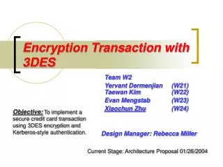
Encryption Transaction with 3DES Team W2 Yervant Dermenjian (W21)Taewan Kim (W22) Evan Mengstab (W23) Xiaochun Zhu (W24) Objective: To implement a secure credit card transaction using 3DES encryption and Kerberos-style authentication. Design Manager: Rebecca Miller Current Stage: Architecture Proposal 01/26/2004
Security In Making Purchases • Identity theft is a growing problem • Sensitive information never transmitted • Uses existing cards and phone network • Credit and charge card fraud costs cardholders and issuers hundreds of millions of dollars each year
Encryption/Decryption Example • Credit #: 2739 8201 4856 2389 Security code: 319 Input Pin # : 4510 key1: 0x32, 0x37, 0x33, 0x39, 0x38, 0x32, 0x30, 0x31 key2: 0x34, 0x38, 0x35, 0x36, 0x32, 0x33, 0x38, 0x39 key3: 0x33, 0x31, 0x39, 0x34, 0x35, 0x31, 0x30, 0xFF • Input : Credit Information • Expiration Date: 08/2008 Plain Text : 0x30, 0x38, 0x2F, 0x32, 0x30, 0x30, 0x38, 0xFF • Output : Cipher Text • 0x2F, 0x81, 0xA8, 0xBF, 0x3C, 0x6B, 0xDF, 0xB4
DES DES-1 DES 3DES Algorithm Flowchart (I) Encryption Cipher Text K3 Plain Text K2 K1 DES-1 DES DES-1 Decryption
3DES Algorithm Flowchart (II) 64 bit plain Text Extension 32 bit 48 bit Left Half Initial Permutation Sub key 48 Bit XOR 16 Rounds Encryption S Box 32 Bit XOR Final Permutation Single Round Right Half cipher Text
3DES Algorithm Flowchart (III) Key Schedule 56bit Key Initial Permutation I=1 I=I+1 Left/Right Half 28 bits Left Barrel Shift N I=16? Final Permutation Y Ready 48 bit Sub-key [ I ]
I/O Pins • Required Inputs: • 32 bits data input at pins • 1 bit reset at pin • 1 bit encryption/decryption mode control at pin • 1 bit clock at pin • Provided Output : • 32 bits data output at pins • 1 bit ready at pin
Block Diagram Key1,3 56’b SRAM 32’b input demux mux Key set Current and next keys 2 x 48’b Register 32’b Key2 56’b SRAM PC-2 (wiring) 56’b 48’b Barrel Shifter 56’b 1’b 16’b ROM I: 0,0,1,1,1,1,1,1,0,1,1,1,1,1,1,0 32’b output 48’b 32’b input IP -1 (wiring) 64’b mux 32’b mux 32’b Plaintext 64’b SRAM PC (wiring) 64’b 32’b mux 32’b XOR R[I] 32’b L[I] 32’b S-box 8x4x16x4’bROM 32’b Expansion 32’b 48’b 48’b P L[I-1] 32’b R[I-1] 32’b XOR 48’b 64’b Register 48’b 32’b 64’b Register
FF FF FF FF S Box {6} {1} 4LUT 16x4bit ROM 4 {1},{6} Mux 4LUT 16x4bit ROM 4 {1:6} Mux {2:5} 4LUT 16x4bit ROM 4 Mux 4LUT 16x4bit ROM
Architecture Analysis • SRAM is used to store the keys and the plain text; 2x48’b registers are used to store the sub-keys during scheduling • Permutation is implemented by wiring • The data input pins are designed to be 32 bits. We need to clock over 2 clock cycles for 64 bits keys; 32 output pins need to clock over 2 clock cycles for the 64 bits cypher text. • The Key schedules can be pinelined with the encryption process. While the key[I-1] is used to encrypt the text, the key[I] will be generated at the same time.
Transistor Estimation (I) • Transistor Count for Key Schedule • 2 x 56 bits SRAM: 672 T • 2 x 28 bits Barrel Shifter: 112 T • 160 X 2-1 Mux/Demux:645 T • 2 x 48 bits Register: 1152 T • PC (4 bit Adder & 4bit Register): 160 T • lookup table(16 bit ROM&4bit Decoder): 104 T • Control Logic: 500 T
Transistor Estimation (II) • Transistor Count for Encryption Process • 1 x 64 bits SRAM: 384 T • 80 bit XOR: 640 T • 8 x S Box (256bits ROM & 6 bit Decoder) : 5728 T • 192 x 2-1 Mux/Demux: 1536 T • 2 x 64 bits Register: 1536 T • PC (4 bit Adder & 4bit Register): 160 T • Control Logic: 500 T • Total Transistor Count:~ 13829 T
Current Status • Design Proposal (100% done) • Architecture Proposal (100% done) • High Level Simulation by C code • Mapping of algorithm into hardware • Behavioral Verilog simulation and test bench • To be done • Floor Plan • Gate-level design • Chip Layout
Design Decisions • Store only 2 keys at a time • Reduce Barrel shifting control values from 1/2 to 0/1 to use only a single bit • Two memory blocks for keys used so Key1 does not have to be inputted twice for Key3
Problems and Questions • Should we choose SRAM or registers to store the sub-keys after scheduling? • The transistors required to store all sub-keys is very large. We hope to be able to only store two sub-keys at a time. • Permutation implemented by wiring may cause messy wire crossover. Can we implement this with logic?