BJT Operation and Analysis in Semiconductor Devices
200 likes | 239 Views
Explore the Ebers-Moll model, base-width modulation, and performance parameters of a BJT in this lecture. Learn to derive terminal currents and analyze emitter, collector, and base regions. Understand how to reduce base-width modulation and calculate the early voltage.

BJT Operation and Analysis in Semiconductor Devices
E N D
Presentation Transcript
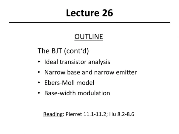
Lecture 26 OUTLINE The BJT (cont’d) • Ideal transistor analysis • Narrow base and narrow emitter • Ebers-Moll model • Base-width modulation Reading: Pierret 11.1-11.2; Hu 8.2-8.6
Notation (PNP BJT) NENAE DEDN tE tn LELN nE0 np0 = ni2/NE NBNDB DBDP tB tp LBLP pB0 pn0ni2/NB NCNAC DCDN tC tn LCLN nC0 np0ni2/NC EE130/230A Fall 2013 Lecture 26, Slide 2 R. F. Pierret, Semiconductor Device Fundamentals, Fig. 11.1
“Game Plan” for I-V Derivation • Solve the minority-carrier diffusion equation in each quasi-neutral region to obtain excess minority-carrier profiles • different set of boundary conditions for each region • Find minority-carrier diffusion currents at depletion region edges • Add hole & electron components together terminal currents EE130/230A Fall 2013 Lecture 26, Slide 3
Emitter Region Analysis • Diffusion equation: • General solution: • Boundary conditions: • Solution: EE130/230A Fall 2013 Lecture 26, Slide 4
Collector Region Analysis • Diffusion equation: • General solution: • Boundary conditions: • Solution: EE130/230A Fall 2013 Lecture 26, Slide 5
Base Region Analysis • Diffusion equation: • General solution: • Boundary conditions: • Solution: EE130/230A Fall 2013 Lecture 26, Slide 6
Since we can write as EE130/230A Fall 2013 Lecture 26, Slide 7
EE130/230A Fall 2013 Lecture 26, Slide 8
BJT Terminal Currents • We know: • Therefore: EE130/230A Fall 2013 Lecture 26, Slide 9
BJT with Narrow Base • In practice, we make W << LB to achieve high current gain. Then, since we have: EE130/230A Fall 2013 Lecture 26, Slide 10 R. F. Pierret, Semiconductor Device Fundamentals, Fig. 11.2
BJT Performance Parameters Assumptions: • emitter junction forward biased, collector junction reverse biased • W << LB Replace LE with WE’ if WE’ << LE EE130/230A Fall 2013 Lecture 26, Slide 11
Ebers-Moll Model increasing (npn) or VEC (pnp) C. C. Hu, Modern Semiconductor Devices for Integrated Circuits, Figure 8-2 • The Ebers-Moll model is a large-signal equivalent circuit which describes both the active and saturation regions of BJT operation. • Use this model to calculate IB and IC given VBE and VBC EE130/230A Fall 2013 Lecture 26, Slide 12
V V EB CB I B E B C I C If only VEB is applied (VCB = 0): aR : reverse common base gain aF : forward common base gain If only VCBis applied (VEB = 0): : Reciprocity relationship: EE130/230A Fall 2013 Lecture 26, Slide 13
In the general case, both VEB and VCB are non-zero: IC: C-B diode current + fraction of E-B diode current that makes it to the C-B junction IE: E-B diode current + fraction of C-B diode current that makes it to the E-B junction Large-signal equivalent circuit for a pnp BJT R. F. Pierret, Semiconductor Device Fundamentals, Fig. 11.3 EE130/230A Fall 2013 Lecture 26, Slide 14
Base-Width Modulation Common Emitter Configuration, Active Mode Operation W IE IC P+ N P + VEB DpB(x) IC (VCB=0) x VEC W(VBC) 0 EE130/230A Fall 2013 Lecture 26, Slide 15
Ways to Reduce Base-Width Modulation • Increase the base width, W • Increase the base dopant concentration NB • Decrease the collector dopant concentration NC Which of the above is the most acceptable action? EE130/230A Fall 2013 Lecture 26, Slide 16
Early Voltage, VA Output resistance: A large VA (i.e. a large ro ) is desirable IC IB3 IB2 IB1 VEC 0 VA EE130/230A Fall 2013 Lecture 26, Slide 17
Derivation of Formula for VA Output conductance: for fixed VEB where xnC is the width of the collector-junction depletion region on the base side xnC P+ N P EE130/230A Fall 2013 Lecture 26, Slide 18
EE130/230A Fall 2013 Lecture 26, Slide 19
Summary: BJT Performance Requirements • High gain (bdc >> 1) • One-sided emitter junction, so emitter efficiency g 1 • Emitter doped much more heavily than base (NE >> NB) • Narrow base, so base transport factor aT 1 • Quasi-neutral base width << minority-carrier diffusion length (W << LB) • IC determined only by IB (IC function of VCE,VCB) • One-sided collector junction, so quasi-neutral base width W does not change drastically with changes in VCE (VCB) • Based doped more heavily than collector (NB > NC) (W = WB – xnEB – xnCB for PNP BJT) EE130/230A Fall 2013 Lecture 26, Slide 20