Download
1 / 23
230 likes | 268 Views
Explore the essential attributes of digital circuits, including voltage ranges, logic swing, noise margins, fan-in/out, rise/fall times, and power dissipation. Learn about binary levels, input/output voltages, noise handling, and propagation delays in digital systems.

E N D
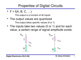
Properties of Digital Circuits • F = f(A, B, C, …) The output is a function of all inputs • The output values are quantized The output takes specific values (0 or 1) • The inputs take two values (0 or 1) and for each value, a certain range of signal amplitude exists. Vin Vout 1 1 VOH VIH VIL 0 VOL 0
Properties of Digital Circuits (Cont.) • The voltage transfer curves for the inverting and non-inverting Digital Circuit. Vout Vout VOH VOH VOL VOL Vin Vin VIL VIH VIL VIH Non-Inverting Circuit Inverting Circuit
Voltages • VOH • Minimum Output Voltage considered to be High. • VOL • Maximum Input Voltage considered to be Low. • VIH • Minimum Input Voltage considered to be High. • VIL • Maximum Input Voltage considered to be low.
Logic Swing and Transition Width • Logic Swing – Magnitude of voltage difference between the output high and low voltage levels. • VLS = VOH – VOL • Transition Width – Amount of voltage change that is required to cause a change in the output voltage. • VTW = VIH – VIL
VCC Vin Vout The Ideal Digital Circuit Element • Operates from a single power source (Vcc) • The two binary levels (0 and 1) are at 0 V and Vcc.
The Ideal Digital Circuit Element • Negligible current drawn from supply source • Output impedance is low => large fan-out is possible. • Transition betweenlogic states occursabruptly atVin = Vcc/2 Vout VCC Vin VCC
Vin Vout t t The Ideal Digital Circuit Element • There is negligible delay between input transition and resulting output transition.
Noise • Noise :- A transient un-wanted variation of voltage or current. • If the magnitude of the noise is large enough, it can cause logic errors. At this point, the output is no longer 0 from the view of the next input VIL VOL
Noise (Cont.) • If the noise amplitude at the input of a logic gate is smaller than its “Noise Margin”, the noise signal will be sharply reduced between the input and the output. • In digital systems, noise does not accumulate from one logic gate to the next.
Noise Margins • “Noise Margin” is the amplitude below which the noise signal will not cause logic errors. • NML(Low Noise Margin) NML = VIL - VOL • NMH(High Noise Margin) NMH = VOH - VIH Vout VOH Vin VOL VIL VIH VOH VOL NMH NML
Typical Inverting Gate Characteristics Vout In this area, the digital circuit behaves like an analog circuit VOH VOL Vin VIL VIH VOH VOL NMH NML
Typical Inverting Gate Characteristics • NOTE: • In the area between VIL and VIH, the digital inverter behaves like an analog device. In that range, the output voltage is a linear amplification of the input voltage. • The amount of time the circuit spends in this range must be minimized as much as possible.
Fan-in and Fan-out • Fan-in – Number of inputs of a particular gate. • Depends on the technology and the functionality of the gate. • Fan-out – Maximum number of inputs that can be connected to a particular output. • Depends on the output’s logic level and the input and output currents.
Fan-out • Logic High Fan-out. • The ratio of the output high current IOH (the current at the output of the gate when the output is high) to the input high current IIH (the current at the input of the gate when the input is high). • Logic Low Fan-out. • The ratio of IOL to IIL • Maximum Fan-out is the minimum of the two values.
Current Directions • Both the input and output currents can flow either into or out of the gate – both in the low and high states. • For fan-out to be possible, the current directions must be complementary. • Fan-out can only be possible if the current flows out of one terminal and into the other.
Vout VOH 90% VLS 10% VOL t tr tf Rise Time and Fall Time
Rise Time and Fall Time • Rise Time (tr): • Amount of time it takes the signal to change from 10% maximum signal value to 90% maximum signal value. • Fall Time (tf): • Amount of time it takes the signal to change from 90% maximum signal value down to 10% maximum signal value.
Vin 50% t tPHL Vout tPLH 50% t Propagation Delays
Propagation Delays • High to Low Propagation Delay (tPHL) and Low to High Propagation Delay (tPLH) • The delay between the time when the input signal passes through 50% of maximum signal value and the output signal passes through the corresponding 50% of the maximum value. • Average Propagation Delay (tP(avg))
Power Dissipation • For the ideal gate, the current drawn from the supply is 0. Therefore, the power usage is also 0. • Practically speaking, every gate has a certain amount of power usage. Moreover, most gates use different amounts of power during transitions (dynamic power dissipation) and during idle states (static power dissipation. • The power dissipation also differs based on the state and the direction of transition.
Power Dissipation (Cont.) • The power consumption is specified as an average or • Some logic families use two power supplies. So, the average power dissipation would be the sum of the average dissipation from each supply. PDISP(avg) = PCC(avg) + PEE(avg)
Power-Delay Product • A measure of the quality of the digital circuit is the product of its power dissipation and the average delay. PD = PDISS(avg) * tP(avg)
Important Factors • Three important factors in the design of any digital circuit: • Physical Size – Determines manufacturing cost. • Power Consumption – Determines operating cost. • Delay – Determines overall performance. • All three need to be as small as possible. However, practically, it is impossible to minimize all three. Therefore, digital circuit design becomes a trade off between the different factors.