Download
1 / 21
420 likes | 1.06k Views
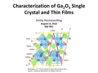
Characterization of Ga 2 O 3 Single Crystal and Thin Films. Emily Hommerding August 13, 2012 NSF REU. Bermudez, V.m . "The Structure of Low-index Surfaces of β-Ga2O3." Chemical Physics 323.2-3 (2006): 193-203 . Ga 2 O 3. Anisotropic Unique in that it is transparent, yet conducting

E N D
Characterization of Ga2O3 Single Crystal and Thin Films Emily Hommerding August 13, 2012 NSF REU Bermudez, V.m. "The Structure of Low-index Surfaces of β-Ga2O3." Chemical Physics323.2-3 (2006): 193-203.
Ga2O3 • Anisotropic • Unique in that it is transparent, yet conducting • Conductivity and transparency are related to the dielectric constant • Dielectric constant not yet determined Bermudez, V.m. "The Structure of Low-index Surfaces of β-Ga2O3." Chemical Physics323.2-3 (2006): 193-203.
XPS : X-Ray Photoelectron Spectroscopy • A sample is put in UHV Cylindrical Hemispherical Analyzer • Incoming x-rays hit the sample X-rays • Electrons leave the sample • Electron’s KE is measured by the CHA Ar Sputter Gun • Argon ions can sputter the sample Sample in UHV
Generation of a Photoelectron hν Vacuum Conduction Band EFermi Valence Band 2p 2s 1s
Conservation of Energy Equation for XPS Energy of the incoming x-ray (k-α of Al) Work function of the spectrometer used to measure kinetic energy Binding energy of the electron in an atom on the surface Kinetic energy of the electron that has been excited from the sample Fadley, Charles S. "X-ray Photoelectron Spectroscopy: From Origins to Future Directions." Nuclear Instruments and Methods in Physics Research Section A: Accelerators, Spectrometers, Detectors and Associated Equipment 601.1-2 (2009): 8-31.
XPS / Sputtering Application Sputter Gun Pd deposited on the surface The Goal: Gradually sputter away a spot of Pd for a future application
XPS Line Scan of the Sputtered Spot 5 x 10 Ga 2p high resolution scan 4 4 x 10 x 10 2.5 Survey Scan 4 16 6 3.5 14 2 6 3 12 2.5 10 1.5 2 c/s c/s 1 8 c/s 1.5 1 6 Pd High resolution Scan 1 1 4 6 0.5 Pd surface coating 2 0.5 0 0 1130 350 1128 348 1126 346 1124 344 1122 342 1120 340 1118 338 1116 336 1114 334 1112 332 1110 330 1 3 2 5 4 6 Binding Energy (eV) Binding Energy (eV) 1 0 Sputtered Spot 1000 900 800 700 600 500 400 300 200 100 0 Binding Energy (eV)
UV Visible Spectroscopy • UV light passes through a sample • A detector lies behind the sample • The percent of light transmitted through the system at a given wavelength is measured and compared with a reference beam Oliva, Brittany L., and Andrew R. Barron. "Connexions." Connexions. Rice University, 5 June 2010. Web. 27 July 2012. <http://cnx.org/content/m34525/latest/>.
Optical Constants, Band Gap Optical Absorption Coefficient Where d is the thickness and The band gap is related to the optical absorption coefficient in the following way
00 Rotations of the single crystal produce differing optical properties!
Ellipsometry Light Source Incident linearly polarized light of known polarization and amplitude is reflected off the top surface of a sample. Reflected light is elliptically polarized and has a change in amplitude Detector Polarizer Variable angle of incidence Analyzer Linearly Polarized Light Incident on Sample Elliptically Polarized Light Leaves Sample Sample "Light & Materials - Part I." Spectroscopic Ellipsometry Tutorial Light and Materials I. J.A. WOOLLAM CO. INC, n.d. Web. 31 July 2012. <http://www.jawoollam.com/tutorial_2.html>.
Optical Properties Index of Refraction The phase velocity of light slows down in a material Dielectric Constant The index of refraction and dielectric constant are related Optical Absorption Coefficient (again) • Ellipsometry can be used to determine.. • Optical constants • Thickness • Composition • Crystallinity The optical absorption coefficient is the same as was used to extract band gap information in UV-Visible Spectroscopy
Phase Amplitude Fresnel Reflectivity Equations Reflected parallel Reflected perpendicular An electric field parallel to the plane of incidence is p-polarized, and perpendicular is s-polarized
Single Crystal Ga2O3Ellipsometry Data at One Orientation Angles refer to angle of incidence Something is ‘turning on’ just under 5eV .. close to Ga2O3’s band gap! • Next steps… • Plot data from other orientations of the single crystal • Use a model to achieve a fit that works for each orientation
Ga2O3 Single Crystal Ellipsometry at Three Orientations Two oscillator models are used to fit the data A relatively good fit for three crystal orientations and three angles of incidence is achieved, and the resulting dielectric constants are plotted
Compare Single Crystal Results to Thin Films Can we differentiate a crystalline Ga2O3 thin film sample from an amorphous one? Films were deposited on a Si substrate, so it is useful to first examine the substrate by itself Dielectric constants of Si from literature Adachi, Sadao. "Model Dielectric Constants of Si and Ge." Physical Review B 38.18 (1988): 12966-2976.
Ga2O3 Thin Film Results Ga2O3 Nominally 100nm thin film deposited on Si; Expected to be amorphous Ga2O3 Nominally 100nm thin film deposited on Si & annealed; Expected to be polycrystalline
Nominally amorphous film Modeled using B-Spline with Kramers-Kronig analysis Thickness = 128 nm Roughness = 9 nm Dielectric Constants Nominally polycrystalline film Modeled using a Psemi M0 oscillator and a Cody Lorentz oscillator Thickness = 156 nm Roughness =13 nm
Conclusion • Ga2O3’s unique properties can be explored for future device applications • XPS is a powerful tool for examining surface and interface features • UV-Vis can measure band gaps and identify anisotropy • Ellipsometry is a quick optical technique which can determine many material properties and optical constants
Acknowledgements A special thanks to Marjorie Olmstead and Fumio Ohuchi for advising me in this project Thanks to Alejandro Garcia and SubhadeepGupta and the NSF for facilitating the REU program