ECE 404
ECE 404. PCB Design Presentation. - Binod Pant. Introduction. Printed circuit board Mechanical support Electrically connect electronic components using conductive pathways, or traces PCB populated with electronic components is a printed circuit assembly (PCA). Why PCB?.

ECE 404
E N D
Presentation Transcript
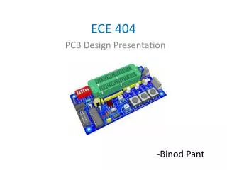
ECE 404 PCB Design Presentation -Binod Pant
Introduction • Printed circuit board • Mechanical support • Electrically connect electronic components using conductive pathways, or traces • PCB populated with electronic components is a printed circuit assembly (PCA)
Why PCB? • Rugged, inexpensive, and can be highly reliable • Faster (due to automation) and consistent in high volume production • Professional(more neater look)
Materials of PCB • Conducting layers are typically made of thin copper foil. • The board is typically coated with a solder mask that is green in color. Other colors that are normally available are blue and red. • Unwanted copper is removed from the substrate after etching leaving only the desired copper traces or pathways
Parts of a PCB • Components • Pads • Traces • Vias • Top Metal Layer • Bottom Metal Layer
Components • Components are the actual devices used in the circuit. • This includes input/output connections. • I/O ports, including power supply connections, are also important in the PCB design.
Pads • Location that components connect to. • You will solder components to the pads on the PCB. • Pads will connect to traces. • Pads have an inner diameter and outer diameter.
Traces • Traces connect pads together. • Traces are essentially the wiring of the PCB. • Equivalent to wire for conducting signals • Traces sometimes connect to vias. • High current traces should be wide. • Signal traces usually narrower than power or ground traces
Vias • Pad with a plated hole connecting traces from one layer of board to other layers. • Attempt to minimize via use in your PCBs. • Some component leads can be used as vias.
Top Metal Layer • Most of the components reside on the top layer • Fewer traces on the top layer • Components are soldered to the pads on the top layer of PCB • Higher circuit densities
Bottom Metal Layer • Few components on this layer. • Many traces on this layer. • Most soldering done on this layer.
Jumpers • Often, many signal wires need to exist in too small of a space and must overlap. • Running traces on different PCB layers is an option. • Multilayer PCBs are often expensive. • Solution: use jumpers
Solder Mask • Protect copper traces on outer layers from corrosion • Areas that shouldn't be soldered may be covered with polymer resist solder mask coating • Designed to keep solder only in certain areas • Prevents solder form binding between conductors and thereby creating short circuits(i.e. hides traces from solder)
Soldering • Wave Soldering- for through hole and SMT • Reflow Soldering- for SMT
Silkscreen • Printing on the solder mask to designate component locations • Readable information about component part numbers and placement. • Helpful in assembling, testing and servicing the circuit board.
Multilayer PCBs • More then a top and bottom layer. • Typically there will be a power plane, ground plane, top layer, and bottom layer. • Sometimes signal layers are added as needed. • Sometimes RF planes made of more expensive materials are added.
Physical Design Issues • Component Size • Heat Dissipation • Input and Output • Mounting Points
Component Size • Make sure components will actually fit. • This especially applies for circuits that require high component densities. • Some components come in multiple sizes. SMT vs Through Hole • Sometimes you can get tall and narrow caps or short and wide capacitors.
Heat Dissipation-Heat Sinks • Heat sink dissipates heat off the component • Doesn’t remove the heat just moves it • Some components may get hot. Make sure you get a large enough heat sink. • Data sheets specify the size of the heat sink • A short circuit may result when two devices share the same heat sink
Mounting Points • The PCB needs to be mechanically secured to something. • Could be the chassis-consist of metal frame on which the circuit boards and other electronic components are mounted. • Could be another PCB/socket on PCB. • Could be attachments to a heatsink.
Parasitics • High frequency circuits • Series Inductance • Shunt Capacitance • Inductive Coupling • Capacitive Coupling
Series Inductance • Not an issue for low frequency circuits(<10 Mhz) • The inductance of a trace may be signifigant. • For power connections, a shunt capacitor is added to counter the series inductance of a long trace. • A capacitor has a low AC impedance source • A 100nF capacitor is often used along with a larger capacitor. 100 nF ceramics have very low impedance at higher frequencies.
Shunt Capacitance • Result of wide wires over a ground plane. • Limits speed of circuits, including digital circuits • Typically insignificant for low performance circuits. • To minimize place a capacitor from voltage to ground
Inductive Coupling • Transfer of energy from one circuit component to another through shared magnetic field • Change in current flow through one device induces current flow in other device • Current flow in one trace induces current in another trace • Minimize the long parallel runs of traces • Run traces perpendicular to each other
Capacitive Coupling • Transfer of energy in electrical n/w due to capacitance between circuit nodes • Minimizing long traces on adjacent layers will reduce capacitive coupling • Ground planes are run between the signals that might affect each other.
Pre-work • Thoroughly simulate your circuit-make sure the circuit worked in simulations • Thoroughly test the prototype-make sure the circuit worked on the bread board • Have all the data sheets handy for every components • Play around with the placement of the components
Simulations • Important to simulate the circuits before building them • Allow margin for component tolerances • Avoid using precise components. e.g a PWM controller that requires exact 10 V DC to work and will fail if there is 10.01V • High performance circuits or SMT devices require PCBs and should be simulated extensively first.
Steps in PCB design 2. Shear Raw Material • Film Generation 3. Drill Holes Industry standard 0.059" thick, copper clad, two sides
Steps in PCB design 4. Electrolus copper 5. Apply Image Apply copper in hole barrels Apply Photosensitive Material to develop selected areas from panel
Steps in PCB Design 6. Strip and Etch 7. Solder Mask • Remove dryfilm, then etch exposed copper • Tin protects the copper circuitry from being etched Apply solder mask area to entire board with the exception of solder pads
Steps in PCB Design 8. Solder Coat 9. Silkscreen Apply white letter marking using screen printing process Apply solder to pads http://www.youtube.com/watch?v=Q6WJqjVleG0&feature=related http://www.advancedcircuits.com/
DesignSoftware • PCB Artist • EAGLE • OrCAD etc Gerber files : describe the images of a printed circuit board (copper layers, solder mask, legend, etc.) as well as the drilling and milling data
Transferring your design to a board • Direct Transfer using marker • "Press-N-Peel" sheets and Variations use of heat • Blender pen • Photolithography use of UV light
WEBSITES • http://www.advancedcircuits.com • How to download the software (EAGLE Layout editor) • Go to http://www.cadsoftusa.com • Click ‘Freeware’ • Click ‘Download’ • Find the correct version (Windows/Linux,English) • Also download Manual and Tutorial
References • PCB Design slides by JakiaAfruz • www.wikipedia.org • www.pcbexpress.com • A Practical Guide to high-speed printed circuit board layout