Download

1 / 12
120 likes | 257 Views
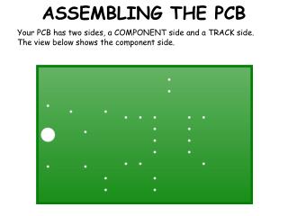
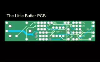
The Little Buffer PCB. K. R6. C3. C. R3. A. A1. TIP. R4. J. D. E. GND. L. F. BRI03. TL071. +V. C2. C1. R1. A3. 0V. R3. H. – V. R2. K. C3. C. R3. A. A1. TIP. R4. J. E. GND. L. F. BRI03. TL071. +V. C2. C1. R1. A3. 0V. R3. H. – V. R2. R6. K. C3.

E N D
The Little Buffer PCB K R6 C3 C R3 A A1 TIP R4 J D E GND L F BRI03 TL071 +V C2 C1 R1 A3 0V R3 H –V R2
K C3 C R3 A A1 TIP R4 J E GND L F BRI03 TL071 +V C2 C1 R1 A3 0V R3 H –V R2 R6
K C3 C R3 A A1 TIP R4 J E GND L F BRI03 TL071 +V C2 C1 R1 A3 0V R3 H –V R2 R6
K C3 C R3 A A1 TIP R4 J E GND L F BRI03 TL071 +V C2 C1 R1 A3 0V R3 H –V R2 Its Labeling R6 D
K R6 C3 C R3 A A1 TIP R4 J D E GND L F BRI03 TL071 +V C2 C1 R1 A3 0V R3 H –V R2 The top traces
K R6 C3 C R3 A A1 TIP R4 J D E GND L F BRI03 TL071 +V C2 C1 R1 A3 0V R3 H –V R2 The bottom traces (viewed from the top – as if the PCB was transparent)
K R6 C3 C R3 A A1 TIP R4 J D E GND L F BRI03 TL071 +V C2 C1 R1 A3 0V R3 H –V R2 LABELING GROUP
K R6 C3 C R3 A A1 TIP R4 J E GND L F BRI03 TL071 +V C2 C1 R1 A3 0V R3 H –V R2