Download
1 / 7
120 likes | 519 Views
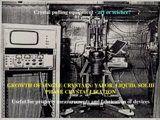
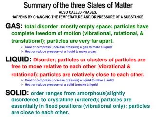
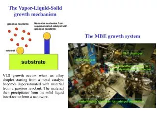
The Vapor-Liquid-Solid growth mechanism. The MBE growth system. III-V chamber. II-VI chamber. XPS chamber for studies on the catalyst-substrate interaction.

E N D
The Vapor-Liquid-Solid growth mechanism The MBE growth system III-V chamber II-VI chamber XPS chamber for studies on the catalyst-substrate interaction VLS growth occurs when an alloy droplet starting from a metal catalyst becomes supersaturated with material from a gaseous reactant. The material then precipitates from the solid-liquid interface to form a nanowire. metallization chamber for catalyst deposition
ZnSe nanowires (Au-catalyzed) (Cd)ZnSe NWs grown at T down to 300 °C (low T necessary for optoelectronics). Best T range 400¸450 °C 1 mm (Ag-catalyzed) Nanotechnology 16, S139 (2005) Appl.Phys. Lett. 86, 153103 (2005)
Mn-catalyzed GaAs NWs on SiO2 on GaAs(110) • No growth on epitaxial GaAs on GaAs(100) High quality NWs between 540 and 620 °C Ø 20-100 nm length: several mm Nano Lett.6, 2130 (2006)
HRTEM on Mn-catalyzed GaAs NWs aMn rich region Wurtzite structure GaAs NWs grown on SiO2 Body: mainly wurtzite + Stacking faults Tip: aMn rich region Nano Lett.6, 2130 (2006)
x 25 x 200 GaAs GaAs:Si GaAs:Be x 1 Charge carriers in GaAs NWs 77 K Au-catalyzed Mn-catalyzed • Undoped GaAs NWs are weakly n-type • GaAs:Si NWs are p-type ?! • GaAs:Be NWs are p-type • Undoped GaAs NWs are p-type • GaAs:Si NWs are n-type • GaAs:Be NWs are p-type Nano Letters 6, 2130 (2006) + Physica E37, 134 (2007).) in press + unpublished
SiO2 ox-GaAs Au-catalyzed GaAs NWs Same growth at Ts = 580 ºC diameter = 20 ÷ 200 nm length = 1 ÷ 5 mm Physica E37, 134 (2007).
mRaman spectra on single Nws • Phonon energy downshift due to the presence of lattice defects • Nearly same structural quality for Mn and Au catalyzed NWs • Raman as a fast tool to statistical screening • (submitted for publication)