Fluid “VLSI”
440 likes | 651 Views
Fluid “VLSI”. System of Channels. Fluidic Systems Ensure Supply and Transport. Bioreactor. Channels. Cross-section: nm to mm range Materials: Glass, silicon, oxide, diamond, polymers Permanently bonded or reversely bondable. PDMS Channels. PDMS is porous and has a hydrophobic

Fluid “VLSI”
E N D
Presentation Transcript
Channels Cross-section: nm to mm range Materials: Glass, silicon, oxide, diamond, polymers Permanently bonded or reversely bondable
PDMS Channels PDMS is porous and has a hydrophobic Hydrophilic properties obtained by surface passivation (O2 plasma, HCL, coating with organic polymers) does not last long. Pour liquid PDMS
Channel Fabrication Processes • Discrete fabrication • channel etch + wafer bonding • materials (etchants): Silicon (EDP, KOH, HNA), glass (HF), molded plastics (various molds including silicon), molded polymer • Monolithic fabrication • sacrificial layer etching for channel fabrication • materials for sacrificial layer: photoresist, oxide • Channel-less microsystems • droplet based microfluid processing
Microfluid Channel Fabrication Technology • Criteria for processing technology • Simplicity of fabrication (hence yield and costs) • Channel material and interior material • compatible with fluid being transported • hydrophobicity • Optical transparency • optical fluid detection is predominant - optical window is required for many concurrent fluid circuits • transparency in visible spectrum, IR, or UV • Geometry constraints • available variety of geometry (depth, width, intersection) • Temperature of processing • Electrical conductivity Ease of fab Materials Optical Geometry Temperature Conductivity Other
Bulk Micromachined Channels • Etch channels in glass or silicon • silica substrate • pyrex glass • photosensitive Foturan glass
Fabrication of Buried ChannelsTjerkstra 1997 * 800 • Step a: Deep reactive ion etching to form channels; • Step b: Low pressure chemical vapor depostion.
Buried Channels (continued …) • Step C: isotropic etching to form the channel; drying of channel solutions; • Step D: deposition of chemical vapor deposition to seal the channels.
Glass Microchips • Jacobson “electrically driven separations on a microchip”, HH’94, p. 65.
Operating Principle • Buffer injection to fill in the entire channel • Analyte injection using electrokinetic flow • Sample introduction and analyte electrophoretic separation • Optical detection is done near the waste port.
Glass Microfabrication Process • (a) starting with glass • (b) deposit and pattern Cr • (c ) use Cr as mask to etch the glass with HF and NH4F bath • (d) remove Cr • (e) bond cover slip. Ease of fab Materials Optical Geometry Temperature Conductivity Other Simple Low cost yes semicircle High T bonding insulator
Silicon Nitride Channels Above SurfacesTjerkstra 1997 * 799 • (a) etching channels in silicon using various techniques to have different shapes; (b) conformal deposition of thin film (e.g. silicon nitride); (c ) anodic bonding of two wafers; (d) etching the top silicon surface.
Merits Ease of fab Materials Optical Geometry Temperature Conductivity Other moderate high moderate varied moderate yes
Parylene Surface Micro Channels Polyimide layer deposited by spin-on Back side Si etching complete (wet or dry etching) Oxide etch (HF) from the back Remove PR
Merits Ease of fab Materials Optical Geometry Temperature Conductivity Other moderate Low Yes one Low Low
Gas Chromatography Channels Silicon channels made by surface micromachining Bonding to glass gives transparency necessary for optical analyzes (absorption at the walls, reaction with dyes etc.) Retention time (transport of species through the column) differ for different species: detection of constituents is possible
Valves and Pumps Low leak rate (ideally, zero leak rate) for fluids and gases Reliable and simple to operate Easy to fabricate Material choice: elastometric polymers (rubber); PDMS is commonly used as soft-membrane material.
PDMS Pneumatic Valves Molding Second molding • thin layer reproduces pattern • thick used for planarization Second PDMS layer used as an upper channel acting as a valve (used for pressure induced by gas or liquid) Two PDMS layers Bonding between two layers in oxygen plasma
Principle of the Microstirrer Schematic of a microstirrer
Micrographs of the Microstirrer SEM pictures of a single microstirrer in a 5x3 array
Passive Mixer • Increase interfacial area to reduce diffusion length • sinusoidal, square-wave, or zigzag channels • divide and conquer approach • lamination-splitting Lamination splitting mixer LIGA micro mixer J. Branebjerg, et al., IEEE MEMS, 1996, p. 442 W. Erhfeld, et al., Ind. Eng. Chem. Res., 1999, 38, p. 1077
Chaotic Advection • Chaotic pathlines can occur and disperse fluid species effectively in smooth and regular flow fields. • Passive mixing using chaos: • 3D serpentine channel • 3D channel made by microstereolithography 3D serpentine channel R. H. Liu, et al., J. MEMS, vol. 9, No 2, June 2000, p. 191 3D mixer made of helical elements A. Bertsch, et al., IEEE MEMS, 2001, p. 508
Active Mixer • Use active perturbation to create time-dependent 2D flows so that chaotic advection can occur • Perturbation can be generated by different sources • vapor pneumatic power • pressure driven • ultrasonic/piezoelectric • electrohydrodynamic convection • electrokinetic flow • mechanical stirring Thermal bubble pump mixer J.-H. Tsai and L. Lin, Transducers ‘01, p. 968
Active Mixing (cont’d) Ultrasonic mixing chamber Z. Yang, et al., IEEE MEMS, 2000, p. 82 Electrohydrodynamic (EHD) convection mixer Mixing by electrokinetic perturbation J.-W. Choi and C. H. Ahn, Solid-State Sens. and Actuator Workshop, 2000, p. 53 Y.-K. Lee, et al., IEEE MEMS, 2001, p. 486
Simulation of Channel Mixing • Simulated by CFDRC fan model • Results can provide a fast way to verify design issues • flow condition • dimension • rotating speed • Mixing vs. rotating speed • increasing micro-stirrer speed can improve mixing Simulation of steady-state channel mixing at (a) rest, (b) 300 rpm, (c) 600 rpm.
Long length make sacrificial layer difficult to remove: use a chevron pattern instead Neuron Probes with Channels Long probes to inject microfluids: sufficient stiffness (penetration neural tissues) and effective supply of fluids (appropriate cross-section). EDP etch (for etching resistance) RIE (mask used) EDP etch deep B diffusion Effective etching for long channels is obtained using porous silicon (Si anodic etching makes porous structure)
18% (a) (a) (b) (c) 750 mm/s 50% (b) 560 mm/s 710 mm/s 86% (c) Flow Sensor Metal wire on glass Channel empty (corresponding to frame (a)) Channel filled (frame (b)) Slope indicates speed
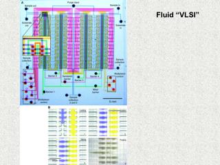
Bio-Barcode Assay in a Microfluidic Chip Control 500 aM 5 fM 50 fM Mean = 10.7 Mean = 28 Mean = 2.18 Mean = 4.9
Empty Fluid Channel Control Channel Silver Staining Filled Fluid Channel Activated Control Channel