Download
1 / 1
70 likes | 600 Views
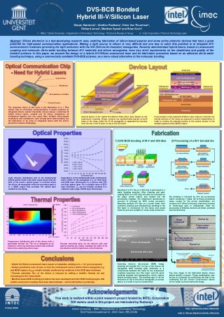
InP top cladding layer. MQW and SCH layers. InP spacer layer. BCB layer. BCB layer. Silicon rib waveguide. Buried oxide (SiO 2 ) layer. DVS-BCB Bonded Hybrid III-V/Silicon Laser. Stevan Stankovi ć 1 , Günther Roelkens 1 , Dries Van Thourhout 1 ,

E N D
InP top cladding layer MQW and SCH layers InP spacer layer BCB layer BCB layer Silicon rib waveguide Buried oxide (SiO2) layer DVS-BCB Bonded Hybrid III-V/Silicon Laser • Stevan Stanković1, Günther Roelkens1, Dries Van Thourhout1, • Richard Jones2, Matthew Sysak2 and Brian Koch2 1 – IMEC / Ghent University – Department of Information Technology - Photonics Research Group 2 – Intel Corporation, Photonic Technology Labs Abstract: Silicon photonics is a fast-developing research area, enabling fabrication of silicon-based passive and some active photonic devices that have a great potential for high-speed communication applications. Making a light source in silicon is very difficult and one way to solve this problem is to integrate III-V semiconductor materials (providing the light emission) with the SOI (Silicon-On-Insulator) waveguides. Recently demonstrated hybrid lasers, based on evanescent coupling and molecular die-to-wafer bonding between III-V materials and silicon waveguides, have very strict requirements on the cleanliness and quality of the bonded surfaces. In this paper, we present the design of a hybrid III-V/Silicon evanescent laser and its fabrication procedure based on an adhesive die-to-wafer bonding technique, using a commercially available DVS-BCB polymer, as a more robust alternative to the molecular bonding. Optical Communication Chip - Need for Hybrid Lasers Device Layout Optical Fiber Multiplexer 25 modulators at 40Gb/s 25 hybrid lasers The long-term vision of this work is the fabrication of a 1 TB/s optical chip for short-haul communications. It would comprise an integrated silicon optical transmitter (shown above) containing 25 hybrid silicon lasers, coupled into 25 silicon modulators, all multiplexed together into one output fiber. Suitable silicon-based modulators and multiplexers have already been demonstrated, but the fabrication of an array of integrated lasers with the silicon photonics remains challenging. General layout of the hybrid III-V/Silicon Fabry-Perot laser based on the evanescent coupling. N-type contacts are symmetrically placed on both sides of the mesa, while the Si rib waveguide is separated by trenches from the rest of the Si layer on top of the SOI wafer. Cross-section of the hybrid III-V/Silicon laser without a thermal via. Lateral sections of the mesa are exposed to proton implantation in order to confine the injected carriers to the central section of the multiple quantum wells (MQW) region. Optical Properties Fabrication 1) DVS-BCB bonding of III-V and SOI dies 2) Processing of a III-V bonded die Light intensity distribution plot of the fundamental hybrid optical mode in the laser cavity shows that the bulk of the mode’s optical power is confined within the silicon rib waveguide, while the secondary peak is in a MQW region that provides the optical gain needed for the lasing. Dependence of the fundamental mode confinement factor within Si rib waveguide (GSi) on SCH layer and BCB layer thicknesses for a device with 230 nm thick spacer layer. For a suitable value of SCH layer thickness, GSi can be virtually constant in a relatively wide range of BCB layer thicknesses. Bonding of a III-V die on a SOI chip is performed in a wafer bonding machine. After cleaning and spin-coating BCB on a SOI chip, the dies are mounted on the glass carrier wafers and loaded into the processing chamber. Die attachment (performed in vacuum) is followed by BCB curing procedure. Mounting multiple III-V dies on a carrier wafer, their collective cleaning and simultaneous bonding to the SOI wafer is envisioned for the future and would make the process suitable for mass-scale production. Die bonding is followed by III-V die processing which comprises 7 steps. All of these processing steps, except for the proton implantation, are carried out in Ghent University cleanroom (located at Technology park in Zwijnaarde). After the processing is finished, devices are diced, polished and characterized. Thermal Properties Thermal via N-type contact pad P-type contact metallization III-V mesa (under the P-type metallization) Temperature distribution plot of the device with a gold-made thermal via. The via is designed as an extension of the top electrical contact and conducts heat to the underlying silicon layer. Thermal resistivity plots for the devices with and without thermal via, clearly visualize the effect of its introduction and the importance of its thickness. Thermal via Conclusions • Hybrid III-V/Silicon evanescent laser, based on InGaAlAs, emitting at λ = 1.31 μm is proposed • Design parameters were chosen so that the confinement factors within silicon waveguide (GSi) and MQW regions (GMQW) remain virtually unaffected by variations in the BCB layer thickness • Thermal resistivity (Rth) of the device is reduced by adding a metallic thermal via and increasing the III-V mesa width • Machine-based BCB bonding procedure has been developed and thin BCB bonding layers that enable evanescent coupling have been demonstrated – device fabrication is underway Scanning electron microscope (SEM) image showing the bonded III-V on top of the silicon rib waveguide. BCB bonding layer thickness is a compromise between the need for the evanescent coupling (requiring very thin layer) and the good bonding strength and planarization which require thicker bonding layers. The bonding layer of 40 nm thickness on top of the silicon waveguide, as shown above, is a result of such a compromise. Top view image of the fabricated device shows plated metallic contacts. P-type metallization also serves as a thermal via conducting the heat to the underlying SOI die. Device cross-section sketch (not to scale) is shown below the image. Acknowledgements This work is realized within a joint researchproject funded by INTEL Corporation SOI wafers used in this project are fabricated by Numonyx mail to: Stevan.Stankovic@intec.UGent.be