Download
1 / 29
320 likes | 570 Views
Nanolitografi. E-beam litografi Nano imprint litografi. Mikroskopi. SEM (scanning electron microscope ). Komponenter i SEM. Schottky emitter elektronkilde. F =-e v x B. Magnetisk linse. E-beam litografi. - Dedikerede e-beam systemer - SEM med Raith Gmbh kontrolsystem

E N D
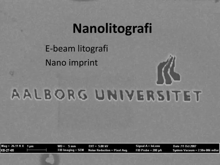
Nanolitografi E-beam litografi Nanoimprintlitografi
Komponenter i SEM Schottky emitter elektronkilde F =-e v x B Magnetisk linse
E-beam litografi - Dedikerede e-beam systemer - SEM med Raith Gmbh kontrolsystem og ’pattern generator’ DANCHIP
Test of nanowire writingE-beam writing+RIE(Nano 9 – Tom+Jeppe)
Optiske strukturer Diffraktive komponenter 2D grating: Periodicity - 250nm
Nanowire detektor Appl. Phys. Lett. 89, 153102 (2006)
Focused Ion Beam Writing As the diagram on the right shows, the gallium (Ga+) primary ion beam hits the sample surface and sputters a small amount of material, which leaves the surface as either secondary ions (i+ or i-) or neutral atoms (n0). The primary beam also produces secondary electrons (e-). As the primary beam rasters on the sample surface, the signal from the sputtered ions or secondary electrons is collected to form an image.
E-beam og FIB litografi • E-beam ~10 nm • FIB ~20 nm • EDX
CVD med FIB stråle Shinji MATSUI