PID meeting
290 likes | 306 Views
PID meeting. Since our last meeting in London : We had a ETD meeting last month @ Cern on Links , DAQ interface, power supplies, radiation, integration.

PID meeting
E N D
Presentation Transcript
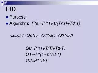
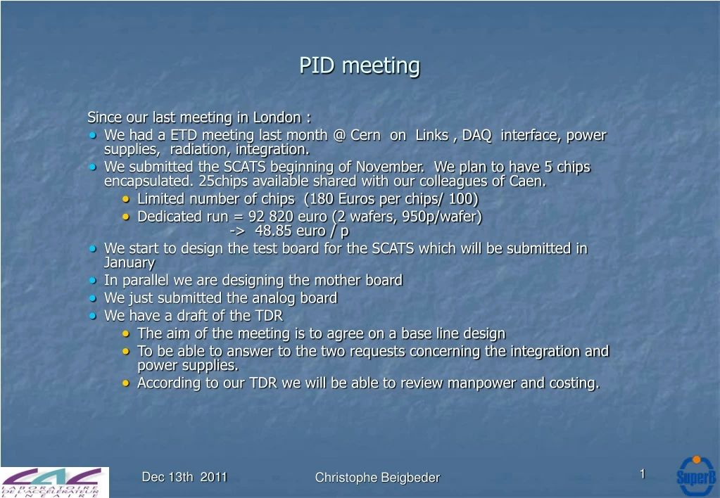
PID meeting Since our last meeting in London : • We had a ETD meeting last month @ Cern on Links , DAQ interface, power supplies, radiation, integration. • We submitted the SCATS beginning of November. We plan to have 5 chips encapsulated. 25chips available shared with our colleagues of Caen. • Limited number of chips (180 Euros per chips/ 100) • Dedicated run = 92 820 euro (2 wafers, 950p/wafer) -> 48.85 euro / p • We start to design the test board for the SCATS which will be submitted in January • In parallel we are designing the mother board • We just submitted the analog board • We have a draft of the TDR • The aim of the meeting is to agree on a base line design • To be able to answer to the two requests concerning the integration and power supplies. • According to our TDR we will be able to review manpower and costing. Christophe Beigbeder
From BABAR toSuperb ~ 10 kPMs / 12 Sectors 12 crates : 14 boards/ 64 channels per board + Concentrator board : serial link to DAQ Commercial crates fasten on the detector Few meters from PM to electronics front end. Channel processing : Time measurement :TDC/ 500 ps bin/250 ps resolution/500 Khz max input rate capability. Charge measurement : 8 bits ADC Christophe Beigbeder
FDIRC FDIRC : new design -> FBLOCK Same bars 12 sectors No more water / sob New PM with Better resolution Higher count rate / channels. 18K/36k channels New requirements : - 200 ps bin - 100 KHz count rate per channel - Trigger rate - Latency - Radiation constraints Christophe Beigbeder
Design option • Two design options : • - A la BABAR : Cables from PM to the Front end electronics. • Crate fixed on the side of the detector or close to it • Pros : Easy access – cooling- Commercial crate. • Cons : Cables cost . S/N ratio . Pick up. Magnetic Field. Shielding. • To be study : Resolution performances after 5 meters long cables with/ without local amplification on PM bases. • Electronics on the FBLOCK. • Pros : Shielded by the doors (Neutrons. Magnetic field). No cables. Better signal to noise ratio. Compact solution. • Cons : Mechanical constraints to fix the boards on the FBLOCK • Dismounting issues : difficult access to the electronics • Thermal constraints : Global heat extraction problems…. • Commissioning ( accessibility ) Christophe Beigbeder
Design option : baseline for TDR • Cable costing : BABAR PM cables 1 M FF. (1998 ) -> ~ 200 K Euros. • Rough estimate of the electronics : 700 K Euros • The pros/cons for an electronics on/off the detector are balanced. • Cable cost is the major argument to choose between the 2 options. • Option 2 – electronics on FBLOCK- is considered as baseline for the TDR Christophe Beigbeder
FBLOCK electronics • Boards are guided like in a crate with rails. It permits to mount/dismount them easily • It copies a crate structure. From price concern we will try to use commercial components : bars , rails … • constraints on the design • PM alignment constraints : PM footprints have to be aligned vertically and horizontally with the same precision used in commercial crates. • To power boards we need a backplane Christophe Beigbeder
Backplane Final design : 6 * 8 PM / FBLOCK 64 -> 32 Channels /PM Christophe Beigbeder
Backplane : many options ! 32 rows 32 Boards / 48 channels 16 rows / 8 backplanes 16 Boards / 96 channels 8 rows / 8 backplanes 8 Boards / 192 channels 16 rows / 1 backplane 16 Boards / 96 channels 8 rows / 1 backplane 8 Boards / 192 channels • Mechanical studies to be done • Max channels / board to evaluate Christophe Beigbeder
Backplane • Version with 1 or 2 connectors / PM / 8 backplanes seems to be the best trade off between complexity , modularity , dismounting issue for PM replacement/ alignment • The HV distribution could be included inside the backplane to avoid daisy chain cables passing over the electronics. • The boards will be powered via the backplane • Connection to the power supply : mechanical issues. Non standard. • The boards need cooling • Air flow , cooling system on the FBLOCK : mechanical issues for fan tray. • The board need to receive / send signals : DAQ- ECS- Clock … • Option with cables / board or signal distributed by backplane Christophe Beigbeder
Links : Raw calculations • The calculation of the number of links L for a given subdetector is based on the following parameters: • N: number of channels [channel] • T: trigger rate [events / s] • E: event size [bits / (event x channel)] • R: link baud rate [bits / (link x s)] • The equation giving the minimum number of links with an optimum multiplexing factor and no concern about detector topology is: • L = N x T x E / R • Some of these numbers are common to the whole experiment: • T = 150 k events / s. • R = 2 Gbits / s (conservative payload ) • For barrel PID numbers are the following: • N = 18,000 channels Christophe Beigbeder
Links : Raw calculations • The calculation of the event size is based on the following parameters: • W: trigger window • H: hit rate per channel [hits / s /channel] • D: mean number of data bits per hit [bits / hit] (includes data formatting and encapsulation) • The equation giving the event size E is the following: • E = W x H x D • For barrel PID (focussing DIRC option), numbers could be the following with asimple BABAR-like TDC option: • W = 200 ns • H = 100 kHz • D = 32 bits • E = 2 E-7 x 1.0 E+5 x 32 = 6.4 E-1 [bits/ (w x channel)] • L = 1.8 E+3 x 1.5 E+5 x 6.4 E-1 / 2 E+9 < 1 link !!! Christophe Beigbeder
Backplane (8 boards/sector) : 2 options • Sector concentrator board : • Clock and controls • ECS ( monitoring. JTAG) • DAQ link • 2nd Backplane ~ 20 Mb serial link to the sector concentrator -> 3 cables per sector Clock and controls : one receiver per board. ECS ( monitoring ctrl. JTAG) : One receiver per board + Data link -> 24 cables/sector Concentrator crate close to the detector. Data packing ( backplane) + ECS receiver + Clock and control receiver + Data link -> 3 cables (redundancy has to be foreseen) Christophe Beigbeder
Electronics is split in two parts : • one directly mounted on the PM base receiving the PM signal and processing it with TDC/ADC • the other one concentrates and pack all the channels to send data to the DAQ Electronics on the detector : Mechanical constraints ->FBLOCK design Thermal constraints -> 200 w per crate to be confirmed Power distribution issues . ->Could use rad hard power supply like LHCb Cables and links Only one link per sector Christophe Beigbeder
FB_Crate Power supply Christophe Beigbeder
TDC : Scats 500 KHz to 2 MHz evts/ch 20 MHz to 110 MHz Christophe Beigbeder
Electronics Chain : 16 Channel processing block diagram FPGA ProsAsic 3 PM pulse • ~ 50 Gb/s. Data pushed • L1 derandomizer here ! Max 100 KHz/ch TDC part Readout part • Derandomizer + parallel to serial output • variable latency Christophe Beigbeder
ASIC ASIC ADC ADC latency latency FPGA How to deal with the proposal Go_back_in_time start_flag, go_back, Mn Fifo “M” 16 Bits !empty COMB Trigger Latency W’ wr_en Mn Mn FSM end wr_en delayed Δt W enable FSM registers Mn Counter ECS L W’ W rd empty 112 Mhz Wr_en 256 Bits Digital Data 17x16 bits Latency Pipeline Data_in Data_out M U X 16 bits 1.8 GBits/s Tx L + W’ Event Buffer to ROM 112 Mhz rd rd Analog Data clk Wr_en X N Extra latency 17x16 bits rd Data_out M U X 16 bits Data_in Analog Data 1.8 GBits/s Tx clk Event Buffer to ROM Christophe Beigbeder 112 Mhz
How to deal with … : Solution one Christophe Beigbeder
How to deal with … : Solution two Christophe Beigbeder
Requirements on fan trays and heat exchanger. • A rough estimation gives : • Fe : 500 mW / 16 Channels • PGA : 1 W / 16 channels • TDC : 500 mW / 16 channels • `+ glue => Total 3 W / 16 channels. • => Sector ( ~ 1.5 kchannels ) = ~ 500 W ( 350 W on Babar/~600 ch) • => 11 kW in total. • From Wiener data sheet • Q = ( 3.1 P) / T • Q= airflow in m3 / h • P = Dissipated power ( W) • T = Temperature change at given air flow • -> 1kW power , a specified difference T = 10 degrees requires a airflow of 300 m3/h 0 Christophe Beigbeder
Power Supply Available now Available 1st Qt 04 Christophe Beigbeder
Modular Floating Power Supply • Power box for 6 modules • Floating Range >10Vminimize DC- ground shift on backplane betweenseparated voltage channels,even when the currents are strongly different • Modules freely combinable for current increasing in parallel or as +/- outputs Christophe Beigbeder
Radiation/ Magnetic field • Fans are the weak point in magnetic field • turbine or shielding • The both power modules worked within specifications up to the fluence 3. 1011 p/cm2, 3 * 14KRad. • No destructive single event occurred. • The CANbus connection worked also fine during the irradiation (the controller board was not in the beam). • The output voltage drifted a little (0.2%) due to temperature effect. • FDIRC will benefit of what we learnt on LHCb : • 3 Voting on registers , state machines, FIFO pointers. • Sensitive components qualified in test beam • Use of Actel FPGA • Power protection on boards ( current monitoring and automatic shut down) • Redundancy on sensitive path Christophe Beigbeder
Questionnaire • Number of electronic channel • Number of tubes • Power dissipated per tube • Volume occupied by the electronics (drawings of electronic modules) • Max tolerable distances between the detectors to the electronic modules • Access frequency on the external electronic per year • Frequency access on the detector per year • Modularity of the electronic unit (housing racks) • Number and size of power cable • Number and size of Read-out cables or fibers • Number and size of slow control Minimum bending radius • Shielding requirements (thermal and electrical) • Information drawings on the cable distribution on the detector geometry • Cooling system. • Requirement of cooling system • Power, flow, temperature and type of fluid • Allowed detector temperature variations • Size of the chiller • Cooling pipes distribution at sub detector ends (drawings) • Describe other requirements that have an impact of the space available like auxiliary equipment, minimum space for accessibility, etc • Describe other requirements that have an impact of the space available like space for the commissioning operations and assembly Christophe Beigbeder
The electronics for the FDIRC can be seen as an upgrade of the electronics of the BABAR DIRC. The new requirements of the experiment (Trigger rate, background, radiation environment) and FDIRC specific requirements (resolution, number of channels and topology) have led to a similar but new design of the electronics chain. The electronics will equip the 18,432 channels of the 12 sectors of the FDIRC. The electronics chain is based on a high resolution/ high count rate TDC, a time associated charge measurement on 12 bits and an event data packing sending event data frames to the data acquisition system (DAQ). The target performance of the overall electronics chain is a time resolution of 100 ps rms. This chain has to deal with a count rate per channel of 100 KHz, a trigger rate up to 150 KHz and a minimum distance between triggers of about 50 ns. The estimate radiation level is of the order of 100 rads per year. The use of radiation tolerant components or off the shelves radiation-qualified components is mandatory. However, the expected energy of the particles may make the latch-up effect almost impossible. Thus only the Single Event Upsets have to be taken into account in the design. The use of Actel family FPGA components has been made for their non-volatile flash technology configuration memories, which are well adapted to radiation environment. Several architectures have been studied which can be summarized has below: - All electronics directly mounted on the FBLOCK. - All electronics mounted next to the detector and linked to the PMs by cables. - A part of it on the detector (the Front end boards) and the other part called “crate concentrator“situated close to the detector, in charge of interfacing with the front-end, reading out event data, packing and sending it to the DAQ. The first solution has been chosen as baseline for the TDR for these 2 main reasons: - The price of the cables (PM to Front end boards) can be estimated to 200 kEuros (1/3 of the price of the overall electronics cost), making this solution too expensive. Moreover, the possible option to have pre-amps on the PM bases doesn’t prevent from having electronics and power supplies on the detector. - The large amount of data per channel leads to have the L0 derandomizer and buffer on the Front end boards. The FCTS receiver could be individually located on each Front end board but the number of cables needed pushes to distribute all the control signals on a backplane. Consequently the board dedicated to receiving and transmitting FCTS signals on the backplane naturally tends to also become the event data concentrator and the link to the DAQ. The baseline design is based on a 16-channel TDC ASIC- offering the required precision of 70 ps rms- embedding an analog pipeline in order to provide an amplitude measurement transmitted with the hit time. Thanks to a 12-bit ADC, the charge measurement will be used for electronics calibration, monitoring and survey purposes. The Front end board FPGA synchronizes the process, associates the time and charge information and finally packs them into a data frame which is sent via the backplane to the FBLOCK control board (FBC). The FBC is in charge of distributing signals coming from the FCTS and ECS, packing the data received from the FE boards to a n-event frame including control bits and transferring it to the DAQ. The TDC chip A former TDC chip offering the requested performances of resolution has already been designed for the SuperNemo experiment. It provides a time measurement with both a high resolution (70 ps RMS) and a large dynamic range (53 bits). The architecture of this chip is based on the Christophe Beigbeder
association of Delay Locked Loops (DLLs) with a digital counter, all of these components being synchronized to a 160 MHz external clock. The SuperB chip – SCATS – will keep the same philosophy but the high input rate requirement lead to a complete re-design of the readout part, in order to minimize the dead time per channel by increasing the data output speed. Instead of the registers and multiplexer which are the bottlenecks of the SuperNemo chip readout, it makes use of an individual FIFO memory per channel in order to derandomize the high frequency bursts of input data. With this architecture, data from the DLLs and the coarse counters are transferred into the FIFO memory within two clock cycles. When the transfer is complete, the channel is automatically reset and ready for the next hit. Simulations of the readout state machine showed an output FIFO data ratecapability of 80 MHz. Time ranges for the DLLs and the coarse counter can be easily customized by adjusting the output data format (16, 32, 48 or 64 bits). Therefore, the chip is suitable for various applications with either high count rate & short integration time or low count rate and long integration time. • Fig. ?: block diagram of SuperB FDIRC TDC chip -SCATS-. • A FIFO depth of 8 words has been selected after simulation with a exponential distribution model of delta time between hits (mean rate ~ 1MHz) applied to inputs. To design this FIFO a full custom RAM has been developed. It permits reducingthe size of the chip and consequently its cost. • The chip is designed using known and proved mitigation techniques to face single event upset (SEU) issues due to the low-level radiation environment. • A first version of the chip without the analog FIFO and the discriminator has been submitted in November 2011. • We plan to submit mid 2012 one chip dedicated to the currently missing parts: • A low walk discriminator receiving the PM outputs and sending logic signal to the TDC part of the chip. • An analog pipeline synchronized with the digital FIFO and providing analog output for charge measurement. Christophe Beigbeder
After testing and validation, a final version of SCATS will then be assembled and submitted end 2013 The front end crate The board input will fit the topological distribution of the PM on the FBLOCK. The PMs are arranged as a matrix of 6 in vertical direction by 8 in horizontal direction. Each column of 6 PMs will fit to one FE board. One vertical backplane (PM Backplane) will interface between the 4 connectors of each PM base to one connector of FE board. The PM backplane is also in charge of distributing the High Voltage, thus avoiding HV cables to pass over the electronics. The FB_ crate will use as much as possible the elements of a commercial crate, in order to avoid the design of too many specific elements like board guides. The FBLOCK equipped with the boards and fan tray Front end crate: PM Backplane – Communication backplane – FE board - FBLOCK controller (FBC Christophe Beigbeder
The communication backplane Distributes the ECS and FCTS signals from the FBC to the 8 FE boards thanks to point to point LVDS links. Connects each FE board to the FBC for data transfer. A serial protocol will be used between FE board and the FBC in order to reduce the number of wires and consequently ameliorate the reliability. The PM Backplane Interface the 6 PMs of a column to one FE board. The 32 channels of each PM distributed on the 4 connectors of the PM base are merged into one connector to get into the Front end connector. It also insures the ground continuity between FE board – crate – FBLOCK. Taking into account the isolation constraints between plans of the printed circuit board, it distributes the High Voltage to the PM base. Cooling and power supply The electronics is located on the detector in a place enclosed by the doors. There are 2 major consequences: one is the problem of the cooling which must be carefully studied in terms of reliability and capability and the second is that the location is “naturally” shielded. Consequently the use of magnetic sensitive components as coils or fan trays is possible. An estimation of the overall electronics consumption lead to 11 kW, non including the HV modules and the power supplies. The cooling system must be designed in order to maintain the electronics located inside at a constant temperature close to the optimum of 30 degrees. The air inside the volume must be extracted while the dry, clean temperature controlled air will be flowing inside. Each FB_ crate will have its own fan tray like in a commercial crate. Targetting a difference of 10 degrees between inside and outside temperature drives to a rough estimate value of 300 m3/h per crate. 4000 m3/h can be considered as the baseline value for the whole detector. The front end board One FE board is constituted of 6 channel-processing blocks handling the 192 channels of one column of PMS. The channel-processing block is constituted bofy 2 SCATS chips, 2 ADCs, one Actel FPGA and some glue logics. The FPGA synchronizes the TDC and the ADC. Upon the reception of L1 trigger, it associates time and charge for the event and packs the data into an event frame. The FE board transfers the event frame in differential LVDS to the FBC via the communication backplane. Christophe Beigbeder