Download
1 / 1
10 likes | 122 Views
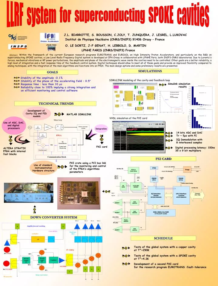
LLRF system for superconducting SPOKE cavities. 3.3 et 1.5V (FPGA). 3.3 et 5V. JTAG. Vregs. PCK111 Clock driver. 80 MHz Clk. +5 et -5V (Analog). -12V. Main loop. INCI_In TRAN_In REFL_In REFC_In. PROM EPC4. PROM EPCS1. Clocks LVPECL. Config FPP. x4. x4.

E N D
LLRF system for superconducting SPOKE cavities 3.3 et 1.5V (FPGA) 3.3 et 5V JTAG Vregs PCK111 Clock driver 80 MHz Clk +5 et -5V (Analog) -12V Main loop INCI_In TRAN_In REFL_In REFC_In PROMEPC4 PROMEPCS1 Clocks LVPECL Config FPP x4 x4 Active Serial Config AD8138 14 bit ADC AD6645 Down converter system I/Q modulator AD8138 14 bit ADC AD6645 AD8138 14 bit ADC AD6645 AD8138 14 bit ADC AD6645 AMPLI 14 IQ Detection Stratix EP1S20 BGA484 cPci Interface Cyclone EP1C4 BGA324 33 MHz Clk 4 Dig_In CompactPCI / PXI I/Q modulator Dig_Out 4 FPGA 14 DAC AD9764 AD8047 PID IQ Demodulation Control and Monitoring ADC DAC Add, Dat, R/W DAC AD9764 14 256k 18bits 4ns RAM CY7C1327F-133AC AD8047 352.2 MHz Feed forward A A A Modul. AD8345 RF_Mod Communication block DAC AD9764 14 AD8047 LPNHE PARIS TECHNICAL TRENDS Development of Cavity IQ and PID models MATLAB SIMULINK Use ofADC, DAC, and digital processors Integration PXI card ALTERA STRATIX FPGA with internal fast blocks Use of standard instrumentation Hardware structure PXI crate using a PCI bus link for the monitoring and control of the FPGA’s algorithms parameters Tests of the global system with a copper cavity at T°=290K Tests of the global system with a SPOKE cavity at T°=4.2K Development of a second PXI card for the research program EUROTRANS :fault-tolerance J.L. BIARROTTE, S. BOUSSON, C.JOLY, T. JUNQUERA, J. LESREL, L.LUKOVAC Institut de Physique Nucléaire (CNRS/IN2P3) 91406 Orsay – France O. LE DORTZ, J-F GENAT, H. LEBBOLO, D. MARTIN LPNHE PARIS (CNRS/IN2P3) France Abstract:Within the framework of the current European research programs EUROTRANS and EURISOL on High Intensity Proton Accelerators, and particularly on the R&D on superconducting SPOKE cavities, a Low Level Radio Frequency Digital system is developed at IPN Orsay in collaboration with LPNHE Paris, both IN2P3-CNRS laboratories. Due to Lorentz's forces, mechanical vibrations or RF power perturbations, the amplitude and phase of the electromagnetic wave inside the cavities need to be controlled. Other goals are a better reliability, a high level of integration and a fast response time of the feedback control system. Digital techniques should allow to meet all of these goals and provide an improved flexibility compared to analog techniques, with the integration of the main algorithms and functions into an FPGA. The main design options and some preliminary results are presented. SIMULATIONS GOALS Stability of the amplitude :0.1% Stability of the phase of the accelerating field : 0.5° Response time : less than 10 µs Reliability close to 100% implying a strong integration and an efficient monitoring and control software SIMULINK modeling of the cavity and feedback loop Simulink simulation results VHDL simulation of the PXI card 14 bits ADC and DAC Tr ~ 5µs with PI IQ Demodulation with 8 interleaved samples Digital processing latency: 100ns 35 x 9 bit multipliers PXI CARD DOWN CONVERTER SYSTEM REFC_In INCI_In REFL_In TRAN_In G G G G A A Amplification and matching Clock 80MHz Band pass filter multiplier SCHEDULE x 8 G IF1 IF=10MHz Ref 10MHz RF1 OL1 Hybrid coupler 90° Combiner Hybrid coupler 90° G OL2 RF2 342.2MHz Ref 352.2MHz A IF2 Image reject mixer RF generator Pi Pt Pr