Download
1 / 33
430 likes | 748 Views
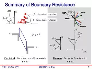
Summary of Boundary Resistance. g(E). E. thermionic emission. f FD (E). tunneling or reflection. ω. ω D,2. µ 1. µ 1 -µ 2 = ?. ω. ω D,1. g( ω ). f BE ( ω ). µ 2. g( ω ). Electrical : Work function ( Φ ) mismatch. Thermal : Debye (v, Θ ) mismatch. ++ ??. ++ ??.

E N D
Summary of Boundary Resistance g(E) E thermionic emission fFD(E) tunneling or reflection ω ωD,2 µ1 µ1-µ2 = ? ω ωD,1 g(ω) fBE(ω) µ2 g(ω) Electrical: Work function (Φ) mismatch Thermal: Debye (v,Θ) mismatch ++ ?? ++ ??
Acoustic vs. Diffuse Mismatch Model Specular Diffuse Acoustic Impedance Mismatch (AIM) = (ρv)1/(ρv)2 Diffuse Mismatch = (Cv)1/(Cv)2 Acoustic Mismatch Model (AMM) Khalatnikov (1952) Diffuse Mismatch Model (DMM) Swartz and Pohl (1989) Snell’s law with Z = ρv (normal incidence)
Debye Temperature Mismatch DMM Stevens, J. Heat Transf. 127, 315 (2005) Stoner & Maris, Phys. Rev. B 48, 16373(1993)
General Approach to Boundary Resistance (conductance) Ex E|| fFD(Ex) A B Flux J = #incident particles x velocity x transmission prob. transmission 0 L More generally: fancier version of Landauer formula! ex: electron tunneling
Band-to-Band Tunneling Conduction • Assuming parabolic energy dispersion E(k) = ħ2k2/2m* • E.g. band-to-band (Zener) tunneling in silicon diode F = electric field See, e.g. Kane, J. Appl. Phys. 32, 83 (1961)
Thermionic and Field Emission (3D) thermionic emission Φ tunneling (field emission) µ1 F µ2 µ1-µ2 = qV field emission a.k.a. Fowler-Nordheim tunneling see, e.g. Lenzlinger, J. Appl. Phys. 40, 278 (1969) S. Sze, Physics of Semiconductor Devices, 3rd ed. (2007)
The Photon Radiation Limit Phonons behave like photons at low-T in the absence of scattering (why?) Acoustic analog of Stefan-Boltzmann constant ci = sound velocities (2 TA, 1 LA) Heat flux: what’s the temperature profile? Swartz & Pohl, Rev. Mod. Phys. 61, 605 (1989)
Phonon Conductance of Nanoconstrictions 1) a >> λ τ = cos(θ) λ = dominant phonon wavelength Prasher, Appl. Phys. Lett. 91, 143119 (2007)
Phonon Conductance of Nanoconstrictions 2) a << λ λ = dominant phonon wavelength Prasher, Appl. Phys. Lett. 91, 143119 (2007)
Why Do Thermal Boundaries Matter? • Because surface area to volume ratio is greater for nanowires, nanoparticles, nanoconstrictions • Because we can engineer metamaterials with much lower “effective” thermal conductivity than Mother Nature TEM of superlattice source: A. Majumdar
Because of Thermoelectric Applications • No moving parts: quiet and reliable • No Freon: clean Courtesy: L. Shi, M. Dresselhaus
Thermoelectric Figure of Merit (ZT) Coefficient of Performance where ZT is… TH = 300 K TC = 250 K Seebeck coefficient Freon (CFCs) Electrical conductivity Bi2Te3 Temperature Thermal conductivity Courtesy: L. Shi
ZT State of the Art Venkatasubramanian et al. Nature 413, 597 2.5-25nm Bi2Te3/Sb2Te3 Superlattices • Goal: decrease k (keeping σ same) with superlattices, nanowires or other nanostructures • Nanoscale thermal engineering! Harman et al., Science 297, 2229 Quantum dot superlattices 5 Courtesy: A. Majumdar, L. Shi
Nanoscale Thermometry Reviews: Blackburn, Semi-Therm 2004 (IEEE) Cahill, Goodson & Majumdar, J. Heat Transfer (2002)
Typical Measurement Approach • For nanoscale electrical we can still measure I/ΔV = AJq/ΔV • For nanoscale thermal we need Jth/ΔT, but there is NO good, reliable nanoscale thermometer • Typically we either: a) Measure optical reflectivity change with ΔT b) Measure electrical resistivity change with ΔT (after making sure they are both calibrated) • Must know the thermal flux Jth
The 3ω Method (thin film cross-plane) • I ~ 1w • T ~ I2 ~ 2w • R ~ T ~ 2w • V3ω~ IR~ 3w Metal line L 2b V Thin film I0 sin(wt) Substrate where α is metal line TCR D. Cahill, Rev. Sci. Instrum. 61, 802 (1990) T. Yamane, J. Appl. Phys. 91, 9772 (2002)
3ω Method Applications… Thin crystalline Si films Ju and Goodson, Appl. Phys. Lett. 74, 3005 (1999) Compare temperature rise of metal line for different line widths, deduce anisotropic polymer thermal conductivity Superlattices Song, Appl. Phys. Lett. 77, 3154 (2000) Ju, Kurabayashi, Goodson, Thin Solid Films 339, 160 (1999)
The 3ω Method (longitudinal) Lu, Yi, Zhang, Rev. Sci. Instrum. 72, 2996 (2001) V I0 sin(wt) Wire • Low frequency: V(3ω) ~ 1/k • High frequency: V(3ω) ~ 1/C • Tested for a 20 μm diameter Pt wire • Results for a bundle of MW nanotubes: • C ~ linear T dependence, low k ~ 100 W/mK Substrate • 3w mechanism: ΔT~ V2/k and R ~ Ro + αΔT
Another Suspended Bridge Approach Multiwall nanotube Pt heater line Pt heater line SiNxbeam Suspended island Source: L. Shi
Measurement Scheme Gt =kA/L T T T s Thermal Conductance: s h QH = IRH t R R h s Tube QL = IRL Environment I T 10 nm multiwall tube 0 VTE Beam Thermopower: Q = VTE/(Th-Ts) Island Pt heater line
Multiwall Nanotube Measurement L. Shi, J. Heat Transfer, 125, 881 (2003) 14 nm multiwall tube Measurement result Cryostat: T : 4-350 K P ~ 10-6torr
Scanning Thermal Microscopy (SThM) • Sharp temperature-sensing tip mounted on cantilever • Scan in lateral direction, monitor cantilever deflection • Thermal transport at tip is key (air, liquid, and solid conduction) TA TT TS Source: L. Shi, Appl. Phys. Lett. 77, 4296 (2000)
SThM Applied to Multi-Wall Nanotube • Must understand sample-tip heat transfer • Note arbitrary temperature units here (calibration was not possible) • Note Rtip ~ 50 nm vs. d ~ 10 nm Source: L. Shi, D. Cahill
Scanning Joule Expansion Microscopy • AFM cantilever follows the thermo-mechanical expansion of periodically heated (ω) substrate • Ex: SJEM thermometry images of metal interconnects • Resolution ~10 nm and ~degree C Source: W. P. King
Thermal Effects on Devices • At high temperature (T↑) • Threshold voltage Vt↓ (current ↑) • Mobility decrease µ ↓ (current ↓) • Device reliability concerns • Device heats up during characterization (DC I-V) • Temperature varies during digital and analog operation • Hence, measured DC I-V is not “true” I-V during operation • True whenever tthermal >> telectrical and high enough power • True for SOI-FET (perhaps soon bulk-FET, CNT-FET, NW-FET) • How to measure device thermal parameters at the same time as electrical ones?
Measuring Device Thermal Resistance ∆T = P × RTH • Noise thermometry • Bunyan 1992 • Gate electrode resistance thermometry • Mautry 1990; Goodson/Su 1994 • Pulsed I-V measurements • Jenkins 1995, 2002 • AC conductance measurement • Lee 1995; Tenbroek 1996; Reyboz 2004; Jin 2001 Note: these are electrical, non-destructive methods
Noise Thermometry Bunyan, EDL 13, 279 (1992) • Body-contacted SOI devices • L = 0.87 and 7.87 µm • tox= 19.5 nm, tSi = 0.2 um, tBOX = 0.42 um • Bias back-gate accumulation (R) at back interface • Mean square thermal noise voltage ‹vn›2 = 4kBTRB • Frequency range B = 1-1000 Hz • Measure R and ‹vn› at each gate & drain bias • T = T0 + RTHIDVD (RTH ~ 16 K/mW)
Gate Electrode Resistance Thermometry Mautry 1990; Su-Goodson 1994-95 • Gate has 4-probe configuration • Make usual I-V measurement… • Gate R calibrated vs. chuck T • Measure gate R with device power P • Correlate P vs. T and hence RTH
Pulsed I-V Measurement Jenkins 1995, 2002 • Normal device layout • 7 ns electric pulses, 10 µs period • Device can cool during long thermal time constant (50-100 ns) • High-bandwidth (10 GHz) probes • Obtain both thermal resistance and capacitance
AC Conductance Measurement Lee 1995; Tenbroek 1996; Reyboz 2004; Jin 2001 • No special test structure • Measure drain conductance • Frequency range must span all device thermal time constants • Obtain both RTH and CTH • Thermal time constant (RTHCTH) is bias-independent gDS = ∂ID / ∂VDS
Device Thermometry Results Summary • High thermal resistances: • SWNT due to small thermal conductance (very small d ~ 2 nm) • Others due to low thermal conductivity, decreasing dimensions, increased role of interfaces Single-wall nanotube Phase-change Memory (PCM) Silicon-on- Insulator FET Cu Via • Power input also matters: • SWNT ~ 0.01-0.1 mW • Others ~ 0.1-1 mW Bulk FET Data: Mautry (1990), Bunyan (1992), Su (1994), Lee (1995), Jenkins (1995), Tenbroek (1996), Jin (2001), Reyboz (2004), Javey (2004), Seidel (2004), Pop (2004-6), Maune (2006).