Download

1 / 27
270 likes | 280 Views
This study delves into methods to boost gain and bandwidth in semiconductor photodetectors, covering key factors such as photoconductivity, photoconductive gain, and photovoltaic detection principles. The text explores the intricacies of detection mechanisms, transit times, diffusion, drift velocity, and carrier conductivities in silicon material. Additionally, it delves into the parameters influencing optimum performance, like absorption lengths, junction capacitance, and electric field calculations for P-I-N diodes and semiconductor junctions. Understanding these concepts can aid in improving the efficiency and effectiveness of photodetection technologies.

E N D
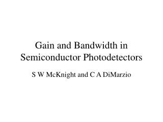
Gain and Bandwidth in Semiconductor Photodetectors S W McKnight and C A DiMarzio
length=l Area=A Photoconductivity Φp = photon flux (photon/sec) η = quantum efficiency
Photoconductor Detectivity and Bandwidth • Sample thickness ~ absorption length • Photoconductive Gain ~ τn • Bandwidth ~ 1/ τn • Gain/Bandwidth product ~ constant
Photovoltaic Detection Jdiffusion E Jdrift Ec Junction “built-in” voltage Vo Ef Ev - + Depletion Region x
Photovoltaic Detection: Gain and Bandwidth • Transit across depletion region fast (vdrift) • Diffusion to depletion region slow (vdiff < <vthermal) • Highest η if absorption is within depletion region • Bandwidth • Transit time of electrons ~ W / (μ ) • Electrical bandwidth ~ 1/RCj • Cj ~ ε A/d ~ 1/W
Diffusion and Drift Velocity Jdiff = q Dn dn/dx = n q vdiff vdiff = Dn 1/n dn/dx = Dn d/dx [ln(n)] ~ Dn ln(gopτ) / (1/α) < < vthermal = sqrt (kT/m) vdrift = μn
Carrier Conductivity Mass Conductivity mass:
Silicon Conductivity Mass b y a c a z x b
Carrier Saturation Velocities Electrons Holes
Photovoltaic Sensing Circuit + Vph -
Photoconductive Sensing Circuit Iph - + Vd
Photoconductive Detection E Jdrift Ec Vo+ Vd Ev Ef - + Depletion Region x
P-N Junction E + - electrons Ef “holes” x Depletion Region
Abrupt Junction ρ P-side N-side qNd -xop xon x -qNa Charge conservation → q Na xop = q Nd xon
Electric Field Calculation Poisson’s Equation: 1D Junction:
Abrupt Junction P-side N-side -xop xon x
P-I-N Junction E + - electrons Ef Ef “holes” x Depletion Region
P-I-N Junction E Ec electrons Ef “holes” Ev - + x Depletion Region
P-I-N Junction P-side I-region N-side xpo xno x ~ Va/W Depletion width = W
Silicon pin diode • W ~ 1/α ~ 10 μ at λ=600 nm • Ebreakdown ~ 106 V/cm • Maximum reverse bias ~ Ebreakdown/W ~ 1000V