Slide Note
0 likes | 11 Views
The project involves designing and testing an analog processing chain for the ICECAL65 particle detector system. Key components include input signal conditioning, gain adjustment, ASIC specifications, rail-to-rail OTA development, and various channel blocks like PZ filters, integrators, and CMOS switches. The focus is on achieving high performance and accuracy for energy measurement in a challenging radiation environment.

E N D
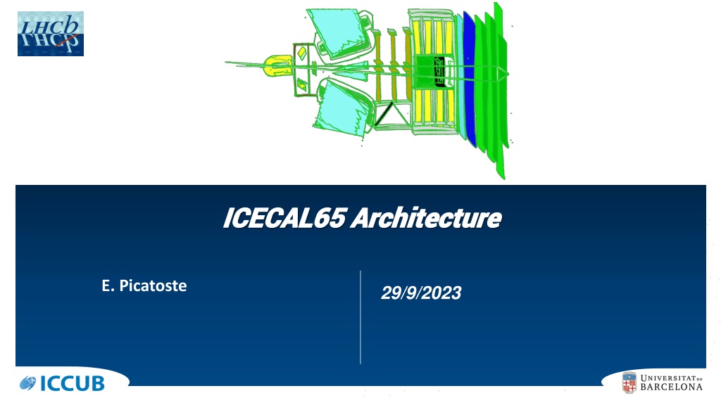
ICECAL65 Architecture ICECAL65 Architecture E. Picatoste 29/9/2023
2 Input signal and gain Front-End ASIC Energy ASIC Digital Back-End Optical Link Detector cells ADC 50Ω I GBT FPGA 12-20m cable PMT Time ASIC ADC Front End Board • Amplifier + Shaper circuit included on the PMT base or FEB under consideration, to compensate cable attenuation, improve SNR, reduce spill-over effort and split the signal between the energy and time paths. • Placement in PMT base only if demonstrated that parts can withstand radiation levels – Radiation tests to be performed on components proposed – 2 stages: transimpedance amplifier + buffer before cable – SE – SE to differential buffer at FEB? • Gain must be defined as 3 different paths are needed: – Time measurement – LG and HG for energy measurement 20 May 2024
3 Input signal and gain (II) Front-End ASIC Digital Back-End Optical Link Detector cells Energ y ASIC ADC 50Ω I GBT FPGA 12-20m cable PMT Time ASIC opamp Front End Board • At FEB – 50 Ohm termination – 2 stages: inverter + SE/differential buffer • ICECAL65 SE vs differential input – SE inputs: half input pins but requires internal SE to differential block – Differential inputs: more robust against noise • HG + LG in chip? – BW↓ – Need of linearity studies 20 May 2024
4 ASIC specifications Energy range(ET): 0 – 10 GeV/c Calibration: High Gain 5 MeV/LSB Low Gain 50 MeV/LSB Dynamic range: 11bit per gain Noise: < 1 LSB Termination: 50 ± 5 Ω Shaping: 25 ns (99% of the charge) Spillover residue level: ±1% Linearity: < 1% Crosstalk: < 0.5% Sampling phase: per channel. • Initial approach: assume similar specifications as ICECAL. • Pedestal subtraction from previous event • Data transmission at 40MHz, continuous readout with no deadtime. 20 May 2024
5 OTA • Development of a Rail-to-rail fully differential OTA in TSMC 65 nm technology to be used • The main specifications that the OTA must achieved are the following ones: TSMC 65nm technology Fully differential Rail-to-Rail (0-1.2 V) Low frequency gain > 70 dB GBW > 500 MHz PM > 65º SR > 0.5 V/ns VCM ~0.6V Power optimization 20 May 2024
6 Analog processing chain Detector cells CHANNEL OUTPUT Track- and-Hold Pre-amp Filter Multiplexer Integrator PMT ADC driver 50Ω ʃ TH PZ I 11b ADC Drv 12b ADC 12b ADC 12b ADC Different lengthes 50Ω ʃ TH PZ x4 ADC clock Integrator clock MEM Track-and-Hold clock Clock Input DLL Front End Board • Input Stage • PZ cancellation Shaper • Integrator • Track & Hold • MUX and output buffer • DLL 20 May 2024
7 ICECAL65 channel blocks: PZ filter Detector cells CHANNEL OUTPUT Track- and-Hold Pre-amp Filter Multiplexer Integrator PMT ADC driver 50Ω ʃ TH PZ I 11b ADC Drv 12b ADC 12b ADC 12b ADC Different lengthes 50Ω ʃ TH PZ x4 ADC clock Integrator clock MEM Track-and-Hold clock Clock Input DLL Front End Board • Pole-zero filter – Different shape signals depending on channel tecnologies, cable and PMT Channel tecnologies: SpaCal W+crystal, Pb+poly, Shashlik Cable: new thinner cables with diferent lengthes depending on the detector zone PMT tr – Try to minimize capacitor value (for OTA) – Adjustable values around expected ones At least ±20% R, C or both 20 May 2024
8 ICECAL65 channel blocks: integrator Detector cells CHANNEL OUTPUT Track- and-Hold Pre-amp Filter Multiplexer Integrator PMT ADC driver 50Ω ʃ TH PZ I 11b ADC Drv 12b ADC 12b ADC 12b ADC Different lengthes 50Ω ʃ TH PZ x4 ADC clock Integrator clock MEM Track-and-Hold clock Clock Input DLL Front End Board • Adjust RC value to reduce C (OTA) • Gain adjust – Variable capacitor 20 May 2024
9 ICECAL65 channel blocks: TH CMOS switches • Precision for 11 bits • High slew rate • Bottom plate sampling technique: → Add fixed ΔQ → fixed charge error (indep of Vi) Hold capacitor clk2 Vin+ + Vo- clk1 Tracking switch - Clock signal generation clk1e Vrefth clk1 FDOA Vo+ clk1e + Vin- - clk1 clk2 Bottom plate sampling technique to minimize non-linearities 20 May 2024
10 ICECAL65 channel blocks: TH clk1 = 1 clk1e = 1 clk2 = 0 (2) Bottom plate off (1) Tracking phase clk1 = 1 clk1e = 0 clk2 = 0 Vin+ + Vin+ + Vo- - Vo- - Clock signal generation FDOA Vrefth FDOA Vo+ + Vo+ + Vin- - Vin- - → Add fixed ΔQ → fixed charge error (indep of Vi) clk1 = 0 clk1e = 0 clk2 = 0 (3) Input switches off (4) Hold phase clk1 = 0 clk1e = 0 clk2 = 1 Vb+ Vin+ + Vo- - + Vo- - FDOA Vo+ FDOA + Vin- Vb- Vo+ - + → Vbx= ct → Q α Vix - 20 May 2024
11 ICECAL65 channel blocks: mux Detector cells CHANNEL OUTPUT Track- and-Hold Pre-amp Filter Multiplexer Integrator PMT ADC driver 50Ω ʃ TH PZ I 11b ADC Drv 12b ADC 12b ADC 12b ADC Different lengthes 50Ω ʃ TH PZ x4 ADC clock Integrator clock MEM Track-and-Hold clock Clock Input DLL Front End Board • 4:1 – One gain → need of a comparator at the input – One of two sub-channels • One output per channel – If one output per several channels, Need higher frequency clock Output buffer needed to cope with ADC parasitic capacitor 20 May 2024
12 Synchronization (previous ICECAL version) Current amplifier CHANNEL OUTPUT Track- and-Hold Filter Multiplexer Integrator PMT signal ADC driver ʃ TH PZ I 12b ADC Drv 12b ADC • Clock management is internally done by the chip • Three clock phases are generated from an input reference (REF_CLK): 1) Track & Hold clock phase (ΦTH). fCLK= 20 MHz. 2) Integrator clock phase (ΦINT= ΦTH+ ΔΦINT). fCLK= 20 MHz. 3) ADC clock phase (ΦADC). fCLK= 40 MHz. • Predictable subchannel selection after reset/power-up. • Internal digitization is also considered but low priority. 12b ADC 12b ADC ʃ TH PZ x4 ADC clock Integrator clock MEM Track-and-Hold clock Clock Input DLL CLOCK INPUT Current Amp output PZ output INPUT PMT signal Main signal TH OUTPUT Tail Main signal CHANNEL OUTPUT Tail 20 May 2024
13 Pinout Aproximated expected number of pins • 2 versions expected: prototype and “final” • Number of channels – Prototype: 4(or less) + parcial channel or blocks? 8? – Final: 8 or 16 • Input channel variations – SE or differential – 1 or 2 gains • Channel outputs: 2 x channel • Other pins: 38+2*channel – Voltage sources, GND, bias, common mode: ~ 29 – Digital (5): 2 x I2C, 1 x RST, 1 x BXI_RST, 1 x Refresh – DLL(4+2*ch): 2 x ctrl, 2 x IN, 2 x channel SE INPUTS INTERNAL GAIN SE INPUTS EXTERNAL GAIN DIF INPUTS INTERNAL GAIN DIF INPUTS EXTERNAL GAIN CHIP PROTO 4x ch 58 PINS QFN64 62 PINS QFN64 62 PINS QFN64 70 PINS QFN80 PROTO o FINAL 8x ch 62 PINS QFN64 70 PINS QFN80 70 PINS QFN80 86 PINS QFN88 FINAL 16x ch 70 PINS QFN80 86 PINS QFN88 86 PINS QFN88 118 PINS BGA144 (?) 20 May 2024
14 Possible packages QFN80 12x12 mm2 QFN64 9x9 mm2 QFN88 10x10 mm2 BGA144 10x10 mm2 20 May 2024
15 Tasks • Define and control common space for ICECAL65 libraries • Define gain at the input: specification • Study OTA with diferent capacitive loads • Gain stage LG/HG in ASIC effect: study linearity • PZ filter adjust to diferent known signal shapes (PZ values) • Switches • Comparator • TH • MUX • Output buffer • Pinout and packaging options study • Commercial ADC available • DLL vs PLL 20 May 2024 SPACAL meeting
16 Thank you for your attention! 20 May 2024
17 Readout architectures: Run 3 (Upgrade I) Front End Board ICECALv3 ASIC Current amplifier Track- and-Hold FRONT-END CRATES Filter Integrator Multiplexer Detector cells ADC driver ʃ PMT TH PZ 50Ω I 12b FPGA 12m cable 12b 12b ADC ADC Drv 12b ADC ADC ʃ clip TH PZ x4 MEM Bias MEM Phase detector charge pump LVDS Clock ADC clock Ref clock CMOS Clock Serial Reg. bus SPI slave MISO, MOSI, !SS, SCLK 25 x4 ME M 20 May 2024