Download
1 / 1
10 likes | 136 Views
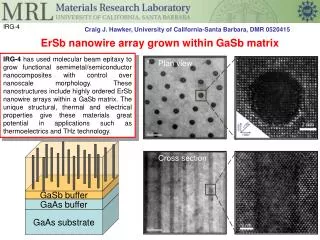
This study by Craig Hawker at the University of California, Santa Barbara, presents the growth of ErSb nanowire arrays within a GaSb matrix using molecular beam epitaxy. The functional semimetal/semiconductor nanocomposites exhibit controlled nanoscale morphology, leading to unique structural, thermal, and electrical properties. These characteristics point to substantial potential in applications such as thermoelectrics and THz technology. Comprehensive analysis includes planar views and cross-sections of the GaSb buffer on GaAs substrates.

E N D
IRG-4 Craig J. Hawker, University of California-Santa Barbara, DMR 0520415 • ErSbnanowire array grown within GaSb matrix IRG-4 has used molecular beam epitaxyto grow functional semimetal/semiconductor nanocomposites with control over nanoscale morphology. These nanostructures include highly ordered ErSbnanowire arrays within a GaSb matrix. The unique structural, thermal and electrical properties give these materials great potential in applications such as thermoelectrics and THz technology. Plan view GaSb buffer GaAs buffer GaAs substrate Cross section