Download
1 / 83
830 likes | 1.13k Views
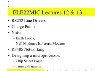
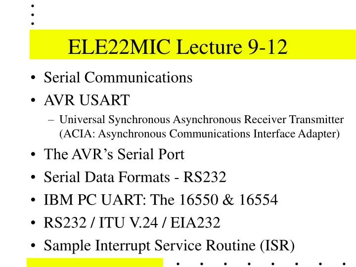
ELE22MIC Lecture 9-12. Serial Communications AVR USART Universal Synchronous Asynchronous Receiver Transmitter (ACIA: Asynchronous Communications Interface Adapter) The AVR’s Serial Port Serial Data Formats - RS232 IBM PC UART: The 16550 & 16554 RS232 / ITU V.24 / EIA232

E N D
ELE22MIC Lecture 9-12 • Serial Communications • AVR USART • Universal Synchronous Asynchronous Receiver Transmitter (ACIA: Asynchronous Communications Interface Adapter) • The AVR’s Serial Port • Serial Data Formats - RS232 • IBM PC UART: The 16550 & 16554 • RS232 / ITU V.24 / EIA232 • Sample Interrupt Service Routine (ISR)
Serial Data Transmission (1) • Serial I/O is the transmission of data over a single communication line. • Cheaper than parallel • Data is moved sequentially one bit at a time. • Requires a conversion from parallel data format to serial format. • This conversion is normally performed by a shift register driven by a clock.
Serial Data Transmission (2) • At the receiving end, data must be reconstructed back into parallel format. • Some method is required to identify bit boundaries. • i.e.: how do you differentiate between 000 and 0000?
Serial communications Devices to perform serial communications have various names - which could be thought of as synonyms: UART: Universal Asynchronous Receiver Transmitter USART: Universal Synchronous Asynchronous Receiver Transmitter ACIA Asynchronous Communications Interface Adapter ACE - Asynchronous Communications Element The UART performs serial-to-parallel conversions on data received from a peripheral device or modem and parallel-to-serial conversion on data received from its CPU. The CPU can read the UART status at any time.
Serial Data Transmission (3) • Two methods: • Synchronous Transmission • Use a common clock to synchronise the receiver with the transmitter. • Therefore requires a separate tine to carry the clock. • Asynchronous Transmission • The receiver and transmitter has separate, independent, accurate local clocks.
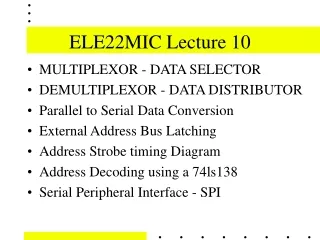
Synchronous Serial Data Transmission(4) • Synchronous Transmission is used with the Serial Peripheral Interface (SPI) • Uses 4 wires: • Clock • Data • Select# • Ground
Serial Peripheral Interface (SPI) During an SPI transfer, data is simultaneously transmitted (shifted out serially) and received (shifted in serially). A serial clock line synchronises shifting and sampling of the information on the two serial data lines. A slave select line allows individual selection of a slave SPI device; slave devices that are not selected do not interfere with SPI bus activities. On a master SPI device, the slave select line can optionally be used to indicate a multiple-master bus contention.
Serial Peripheral Interface (SPI) The SPI can be used to add an extra 8 bit output port using an 8-bit shifter and latches. MasterOutSlaveIn MOSI (Serial Data) -> Pin14 (MSB sent first) Clock ->Pin 11 SS# = Pin 12 = Low during transmission Reset# = Pin 10 = 5V OE# = Pin 13 = 0V
Serial Peripheral Interface (SPI) From ATMEGA128 Manual Page 164
AVR SPI Control Bits • Refer PP151-157 - Embedded C Programming, see also P167 of ATMEGA128 full datasheet. • SPCR - SPI Control Register • SPIE - SPI Interrupt Enable Mask Bit (1 = enable) • SPE - SPI Enable = 1 to enable SPI • DORD - Data ORDer Bit If DORD = 0, SPI transmits MSB first, else (DORD = 1) transmits LSB first
AVR SPI Control Bits • CPOL - Clock Polarity • CPHA - Clock Phase - determines if data is latched on the Leading Edge (0) / Trailing (1) edge of SCK • SPR1:SPR0 Spi PRescaler (SPI Frequency) • 00 = System clock divided by 4 • 01 = System clock divided by 16 • 10 = System clock divided by 64 • 11 = System clock divided by 128
Asynchronous Serial Data Transmission(1) • RS232 Voltage Levels & Data Format • Line Transceiver with Charge Pump - • the MAX232 series. • Serial Data Format • Start Bit, Data Bits, Parity, Stop Bits • Errors: Framing, Overrun, False Start • The 6850 ACIA (Asynchronous Communications Interface Adapter) • AKA: UART (Universal Asynchronous Receiver Transmitter) or ACE (Asynchronous Communications Element) • The RS232 Transmission Distance Limits
USART - Control and Status There are two identical USARTS in the ATMEGA128. Each USART has three control & status registers labelled UCSRnA, UCSRnB and UCSRnC, where n is 0 for USART0 or 1 for USART1. I.e. The Status Register for USART 0 is UCSR0A, UCSR0B and UCSR0C, and USART 1 is UCSR1A, UCSR1B and UCSR1C.
UCSRnA • RXCn is a flag set when data is received. • TXCn is a flag set when the data frame has been sent. • UDRE is a flag set when the User Data Register is Empty • FEn - Framing Error • DORn - Data OverRun - (Data has been lost) • UPEn - Is set to one if the received character had Parity Error • U2Xn - Double the USART transmission speed • MPCMn - MultiProcessor Communication Mode - • When the frame-type-bit (the 9th bit) is set to one, the frame contains an address. When the frame type bit is zero the frame is a data frame. In this mode, the address frames only are received, data frames are discarded unless the address previously matched.
UCSRnB • RXCIEn RX (Receive) Character Interrupt Enable. • TXCIEn TX (Transmit) Character Interrupt Enable • UDRIE - User Data Interrupt Enable • RXENn - Set - enables the USARTn Receiver. • The Receiver will override normal port operation for the RxDn pin when enabled.
UCSRnB • TXENn - enables the USARTn Transmitter. • The Transmitter will override normal port operation for the TxDn pin when enabled. The disabling of the Transmitter (writing TXENn to zero) will not become effective until ongoing and pending transmissions are completed. • • RXB8n: Receive Data Bit 8 - is the ninth data bit of the received character.. Must be read before reading the low bits from UDRn. • • TXB8n: Transmit Data Bit 8 - is the 9th data bit in the character to be transmitted when operating with serial frames with 9 data bits. Must be written before writing the low bits to UDRn.
UCSRnC There are two identical USARTS in the ATMEGA128. Each USART has three control & status registers labelled UCSRnA, UCSRnB and UCSRnC To indicate that the registers naming is the same, the letter n is used where a 0 (for USART0) or 1 (for USART1) would be. Status Register C - UCSRnC. I.e. Status Register for USART 1 is UCSR1C
USART - Data Frame Format The AVR USART can transmit and receive 30 various combinations: 1 start bit; 5 to 9 data bits; even, odd or no parity, and 1 or 2 Stop bits.
USART - Data Frame Format The three bits - USART Character SiZe (UCSZ2:0) - select the number of data bits in the frame.
USART - Transmit The USARTn Transmit Data Buffer register and USARTn Receive Data Buffer Registers share the same I/O address referred to as UDRn (USARTn Data Register n). The Transmit Data Buffer Register (TXBn) will be the destination for data written to the UDRn Register location.
USART - Transmit The transmit buffer can only be written when the UDREn flag in the UCSRAn Register is set. Data written to UDRn when the UDREn flag is not set, will be ignored by the USARTn Transmitter. When data is written to the transmit buffer, and the Transmitter is enabled, the Transmitter will load the data into the Transmit Shift Register when the Shift Register is empty. Then the data will be serially transmitted on the TxDn pin.
USART - Transmit & Receive Reading the UDRn Register location will return the contents of the receive data buffer register (RXBn). The receive buffer consists of a two level FIFO. The FIFO will change its state whenever the receive buffer is accessed. Due to this behavior of the receive buffer, do not use read modify write instructions (SBI and CBI) on this location. Be careful when using bit test instructions (SBIC and SBIS), since these also will change the state of the FIFO.
USART0 & USART1 Config UART0 Control and Status Registers: UART1 Control and Status Registers:
Clock Synchronisation (1) • The receiver phase locks its local clock to the transmitter's clock by detecting the start bit and stop bits of a serial frame. • Thus it does not require a separate clock line as the data line contains timing information. • If the data is sampled in the mid-point of each bit the clock error less than to 5% can be tolerated with communication remaining error-free between transmitter and receiver.
Clock Synchronisation (2) • Start bit signifies the beginning of the frame • Stop bit(s) identify the end of the frame • If the stop bits are received incorrectly it is assumed that the receiver’s clock has drifted out of phase, or some other error has occurred, and a FRAMING ERROR is declared
Communication Terminology • The rate at which data is transmitted is called the bit-rate • Bit-rate is measured in bits per second. • Baud rate refers to the rate per second of the bit symbols used to transmit the serial data. • i.e.: Baud Rate includes the synchronisation items: start bit & stop bit(s). For example: If using 10 bit symbols per 8 bit character at 9600 baud equates to a bit rate of 7680 data bits per second (or 960 Bytes per second).
Serial Data Bit Error Detection • In any data transfer there is the potential for bit-errors. Parity can be used as a check that the correct bit pattern is received. • Parity calculation involves adding the “1” bits in a frame together. • Even Parity • Adding all bits in frame + parity_bit => ‘0’ • Odd Parity • Adding all bits in frame + parity_bit => ‘1’
Bit Error Rate (BER) (1) • The Bit Error Rate - Probability of bit error - is the number of bit errors measured at the receiver through a communication system. The transmission channel may be Radio, Optical Fibre, Copper Cable, etc. • In analog communications the important unit of measure is the Signal to Noise ratio. • These measures are useful to characterise a system and can be measured or simulated.
Bit Error Rate (BER) (2) • If the quality of the system is high, the single bit error rate may be measured in years. In this case a single parity bit would be sufficient to determine data errors & re-transmission could recover the correct data. • The probability of double-bit errors would become negligible. Double-bit errors cannot be detected using a single parity bit.
Improving Noise Immunity • One way of improving noise immunity: sample multiple times through each bit and at each sample time, check the status of each bit. Take the most common value of the sample as the bit value.
USART Syncyronous/Asynchronous The USART supports four modes of clock operation: 1. Normal Asynchronous, 2. Double-Speed Asynchronous, 3. Master Synchronous, and 4. Slave Synchronous mode. The UMSEL bit in USART Control and Status Register C (UCSRC) selects between asynchronous and synchronous operation. Double speed (Asynchronous mode only) is controlled by the U2X found in the UCSRA Register. When using Synchronous mode (UMSEL = 1), the Data Direction Register for the XCK pin (DDR_XCK) controls whether the clock source is internal (Master mode) or external (Slave mode). The XCK pin is only active when using Synchronous mode.
USART Clock Signals Signal descriptions: txclk Transmitter clock. (Internal Signal) rxclk Receiver base clock. (Internal Signal) Slave Synchronous mode operation only: xcki Input from XCK pin (internal Signal). Master Synchronous mode operation only: xcko Clock output to XCK pin (Internal Signal). fosc XTAL (Crystal) pin frequency (System Clock).
USART Transmit Character Code The following code examples show a simple USART transmit function based on polling of the Data Register Empty (UDRE) flag. When using frames with less than eight bits, the most significant bits written to the UDR are ignored. The USART has to be initialised before the function can be used. For the assembly code, the data to be sent is assumed to be stored in Register R16
USART Transmit Complete Flag The Transmit Complete (TXC) flag bit is set one when the entire frame in the Transmit Shift Register has been shifted out and there are no new data currently present in the transmit buffer. The TXC flag bit is automatically cleared when a transmit complete interrupt is executed, or it can be cleared by writing a one to its bit location. The TXC flag is useful in half-duplex communication interfaces, like RS485, where a transmitting application must enter receive mode and free the communication bus immediately after completing the transmission.
USART Parity Generator The parity generator calculates the parity bit for the serial frame data. When parity bit is enabled (UPM1 = 1), the transmitter control logic inserts the parity bit between the last data bit and the first stop bit of the frame that is sent.
USART Parity Generator The parity bit is calculated by performing an exclusive-or of all the data bits. If odd parity is used, the result of the exclusive or is inverted. If parity is disabled, UPM1=0, then no parity bit is transmitted.
Serial Data Bit Sampling • The signal is sampled by the ACIA in the middle of each bit period.