Download
1 / 19
190 likes | 209 Views
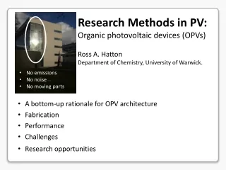
Research Methods in PV: Organic photovoltaic devices (OPVs) Ross A. Hatton Department of Chemistry, University of Warwick. No emissions No noise No moving parts. A bottom-up rationale for OPV architecture Fabrication Performance Challenges Research opportunities.

E N D
Research Methods in PV: Organic photovoltaic devices (OPVs) Ross A. Hatton Department of Chemistry, University of Warwick. • No emissions • No noise • No moving parts • A bottom-up rationale for OPV architecture • Fabrication • Performance • Challenges • Research opportunities
Organic semiconductors Chlorophyll Cu phthalocyanine Tang, Appl. Phys. Lett. 48 (1986) 183. • Earth abundant elements • (cheap, non-toxic) • Strong absorbers • Tuneable properties • (optical, electronic, processing) Meiss et al., Adv. Funct. Mater., 22 (2012) 405. ‘Dial-a -semiconductor’
Organic semiconductors - a world of coulombic interactions Coulomb’s Law: r -q +q Hopping transport Vacuum Level LUMO Eg Energy HOMO Molecular Orbital (MO) Core Levels (AOs) Nuclei Isolated Molecule Molecular (VdW) Solid Vacuum Level – just outside solid surface where electron is at rest. HOMO = Highest occupied MO; LUMO = Lowest unoccupied MO
Organic photovoltaics (OPV) – device architecture • Low charge carrier mobility large electric field (F) needed for extraction. • so for low film thickness (d), can easily achieve required F. * d 200 nm • >100× thinner than c-Si • Advantages associated with ‘thin film’. • Positive temperature coefficient. *Figure from http://www.easac.eu/fileadmin/docs/Low_Carbon/KVA_workshop/Renewables/2013_09_Easac_Stockholm_Leo.pdf
It’s good to be flexible • Weak intermolecular interactions in molecular solids impart flexibility. • Why is flexibility important? • Compatibility with roll-to-roll fabrication (rapid fabrication low cost) • Compatible with light weight substrates (i.e. plastics) – typically flexible. • New applications possible (e.g. integration with fabrics).
- + - + Excitations in molecular semiconductors Excitons = lattice site Exciton diffusion length 10 nm Crystalline inorganic semiconductor Molecular semiconductor • Frenkelexciton • r =2-4 • Binding energy > 0.2 eV • Mott-Wannier exciton • r =10-15 • Binding energy < 25 meV Architecture must: (1) split excitons; (2) Overcome diffusion length limitation.
Splitting excitons into free electrons and holes • Efficient exciton dissociation can be achieved at an organic heterojunction Tang, Appl. Phys. Lett. 48 (1986) 183. S +H LUMO (Fermi level) (Fermi level) Electron donor HOMO Electron acceptor
Splitting excitons into free charge carriers e- e- -3.4 -4.2 SubPc SubPc F6-SubPc C60 -5.5 SubPc C60 -6.2 • Rapid photo-induced electron transfer (100 fs), long lived charge separated state (ms). • From donor to acceptor, by design: e- -3.6 -5.8 F6-SubPc Sullivan, et al., Advanced Energy Materials (2011) 1, 352–355.
Summary of fundamental processes • Light absorption to form an exciton. • Exciton diffusion to the heterojunction. • Exciton dissociation at the organic heterojunction. • Charge carrier transport to electrodes. • Charge carrier extraction.
Donor Acceptor The exciton diffusion bottleneck • Exciton diffusion length in organic semiconductors 10 nm. • Photoactive layer must be structured to accommodate this: Bi-layer Bulk-heterojunction (BHJ) Opaque electrode Transparent Electrode Thin film (high electric field) Organic hetero-junction (split excitons) Interpenetrating heterojunction (overcome limitation in exciton diffusion length)
Processing (vacuum processing) Solution Processing Area Solar Simulator Evaporation Chamber • High purity • High degree of control over layer thickness ( 0.1 nm) • Multi-layer architectures possible • High capital outlay • Energy intensive (high vacuum (10-6 mbar) needed)
Processing (solution processing) Spin coating Spray deposition Printing * Spin-coating (wasteful) minimal loss & scalable to large area • Low cost equipment. • Low embodied energy (no vacuum required) / short payback time. • Difficult to make bilayer architectures. • Simple to make BHJ (spontaneous donor/acceptor phase separation). * Picture from Advancing spray deposition for low-cost solar cell production K. Xerxes Steirer, et al., 25 March 2009, SPIE Newsroom. DOI: 10.1117/2.1200903.1555
Solution processable organic semiconductors • Chemical modification: • Semi-conducting polymers: Eg Eg Homo-polymer Alternating co-polymer
Efficiency evolution Target: efficiency >15%, > 20yr lifetime and low cost Figure adapted from www.orgworld.de
Challenges: Improving efficiency • Narrow band gap organic semiconductors. Donor Acceptor Maximum Voc • Semiconductors that can be processed from non-toxic solvents. • Materials amenable to rapid processing.
Challenges: improving stability • Photo-stability of organic semiconductors • (Materials for OLEDS > 1 millions hours lifetime) • Interface stability (delamination at soft contacts) • Blocking water/oxygen ingress • (particularly challenging on flexible substrates) Photograph by P. Sullivan, University of Warwick.
Challenges: Reducing materials cost • Need for low cost, transparent, flexible electrode. * Photograph from Hatton research group, University of Warwick.
Concluding remarks • OPVs are an emerging thin film PV technology which is potentially very low cost and compatible with flexible substrates. • OPVs are fundamentally different from c-Si PV in the mode of operation and device architecture. • The challenges in this field of research are multi-faceted and inherently interdisciplinary. * Photograph by R. da Campo, Molecular Solar Ltd.
Rises > 2oC look likely, unless there is a real international appetite to change emission paths, and quickly.