DSP56800E Family
210 likes | 440 Views
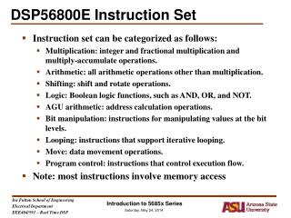
DSP56800E Family. 56858 Features. 40KW Prog RAM. 24KW Data RAM. 1KW Boot ROM. External Memory I/F. 56800E Core 120 MIPS 120 MHz. 6 CH DMA. ESSI0. ESSI1. 2-SCI. SPI. 8-bit Host I/F. Quad Timer. COP. TOD. JTAG/EOnCE. 120 MIPS at 120 MHz 40K x 16-bit Program RAM

DSP56800E Family
E N D
Presentation Transcript
DSP56800E Family Introduction to 5685x Series
56858 Features 40KW Prog RAM 24KW Data RAM 1KW Boot ROM External Memory I/F 56800E Core 120 MIPS 120 MHz 6 CH DMA ESSI0 ESSI1 2-SCI SPI 8-bit Host I/F Quad Timer COP TOD JTAG/EOnCE • 120 MIPS at 120 MHz • 40K x 16-bit Program RAM • 24K x 16-bit Data RAM • 1K x 16-bit Boot ROM • 21 External Memory Address lines, 16 data lines and four chip selects • Six (6) independent channels of DMA • Two (2) Enhanced Synchronous Serial Interfaces (ESSI) • Serial Port Interface (SPI) • Two (2), Serial Communication Interfaces (SCI) • 8-bit Parallel Host Interface • General Purpose 16-bit Quad Timer • JTAG/Enhanced On-Chip Emulation (EOnCE) for unobtrusive, real-time debugging • Computer Operating Properly (COP)-- Watchdog Timer • Time of Day • 144 LQFP and MBGA packages • Up to 47 GPIO Introduction to 5685x Series
Packaging • DSP56858 comes in two packages • 144 pin LQFP (low Profile Quad Flat Oackage) • 144 pin MAPBGA (Mold Array Process-Ball Grid Array) LQFP MAPBGA Introduction to 5685x Series
DSP56858 Block Diagram Introduction to 5685x Series
DSP56858 Pins • Some Ports have dual Function: • Can be programmed to act as a General Purpose I/O (GPIO) or • A hardwired specific function (i.e: ESSI, HPI, SCI…etc. Introduction to 5685x Series
DSP56858 Memory Map • Three Address Busses: • Program memory Address Bus (PAB) – 24 bit • Primary Data Address Bus (XAB1) – 21bit • Secondary Data Address Bus (XAB2) – 21 bit • Data Buses • Data transfers inside the chip occur over the following buses: • Two unidirectional 32-bit buses: • Core Data Bus for Reads (CDBR) • Core Data Bus for Writes (CDBW) • Two unidirectional 16-bit buses: • Secondary X Data Bus (XDB2) • Program Data Bus (PDB) • IPBus interface A 64-word block is allocated in data memory for memory-mapped peripherals registers and can be located anywhere in data memory. The top 12 locations of this block are reserved for use by the DSP core. The I/O short address mode X:<<pp can be used. Introduction to 5685x Series
GPIO Programming Example –Port D • 0 = GPIO mode; pin operation is controlled by GPIO registers • 1 = Normal mode; pin operation is controlled by peripheral module Introduction to 5685x Series
GPIO Programming Example –Port D • 0 = Pin is an input; pull-ups are dependent on value of PUR registers (default) • 1 = Pin is an output; pull-ups are disabled These bits control the output data when in GPIO mode. • 0 = Pull ups disabled for inputs • 1 = Pull ups enabled for inputs (default) Pull ups are automatically disabled for outputs in both modes. Introduction to 5685x Series
Interrupt Controller (ITCN) • The interrupt controller module is used to arbitrate amongst the various interrupt request and to signal to DSP core when an interrupt of sufficient priority exists and what address to jump to in order to service this interrupt • The interrupt controller module performs: • Assign priority level for each interrupt request • Manage two fast interrupts • Notify DSP core to restart clocks out of WAIT and STOP mode Introduction to 5685x Series
Standard Interrupt Arbitration Priority Level Select Bits Priority Level Select Bits Priority Level Select Bits Priority Level Select Bits Priority Level Select Bits Interrupt Request Vector Table Address New Interrupt Priority Level Interrupt Mask Bit Interrupt Arbiter I1 I0 Illegal Instruction Priority Level 3 Arbiter Priority Level 2 Arbiter Priority Level 1 Arbiter Priority Level 0 Arbiter Lowest Priority SWILP Instruction SWI #3 SWI #2 SWI #1 SWI #0 HWS Overflow Misaligned Data Access ... ... If Priority level select Bits is set to 00, the interrupt is disabled BKPT_U0 IRQB SCI1_RCV TPBUF IRQA Interrupt Controller EOnCE Interrupt Sources Peripheral Interrupt Sources • EOnCE Interrupt Sources can be assigned to priority level 3, 2, and 1. • Peripheral Interrupt sources can be assigned to priority level 2, 1, and 0. • Any interrupt sources can interrupt Lowest-Priority Software Interrupt (SWILP interrupt). Introduction to 5685x Series
5685x External Memory Interface • Features: • Access up to 2M words of program and 2M words of data memory • Four Programmable Chip Select Logic • Glue-less interface to ROM, EPROM, Flash EPROM and SRAM etc. • 16-bit data bus • 21-bit address bus (24-bit max for 56800E core) • Support devices with access times up to 250ns. Introduction to 5685x Series
Host Interface (1/2) HOST INTERFACE BUS Interrupt Vector Register DSP INTERNAL BUS Command Vector Register HD[0:7] Interface Control Register Host Status Register HACK/HRRQ Interface Status Register Host Control Register HREQ/HTRQ 8 Receive High Register (RXH) 16 HRW/HRDS Host Transmit Register (HTX) 8 Receive Low Register (RXL) 8 HDS/HWRS Transmit High Register (TXH) 16 Host Receive Register (HRX) 8 Transmit Low Register (TXL) HCS Address Decode HA[0:2] Introduction to 5685x Series
Host Interface (2/2) • Byte-wide, full-duplex, double buffered, parallel port • Operate asynchronously to the DSP core clock • Data transfers are manageable • The host side registers are accessible to the external host processor • The DSP side registers are accessible to the DSP core • DSP Side. • Registers are directly mapped into four X data memory locations. • 16-bit data wide • Transfer mode • DSP to host • Host to DSP • Host Command • Handshaking protocol • Software Polled • Interrupt driven • DMA accesses • Instructions • Memory-mapped registers allow the standard MOVE instruction to be used • Bit manipulation instructions simplify I/O service routines • Host Side. • 16 signal pins are provided to support non-multiplexed data bus • 8-bit data wide • Transfer mode • DSP to Host: 8-bit or 16-bit • Host to DSP: 8-bit or 16 bit • Host Command • Handshaking protocols • Software Polled • Interrupt driven • DMA accesses • Separate interrupt lines for each interrupt source • Special host commands force the host command associated DSP core interrupts under host processor control, which are useful for: • Real-time production diagnostics • Debugging window for program development Introduction to 5685x Series
Enhanced Synchronous Serial Interface (ESSI) • Independent (asynchronous) or shared (synchronous) transmit and receive sections with separate or shared internal/external clocks and frame syncs • Normal mode operation using frame sync • Network mode operation allowing multiple devices to share the port with as many as thirty-two time slots • Network mode enhancements • Time slot mask registers (receive and transmit) • End of Frame Interrupt • Gated Clock mode operation requiring no frame sync • Programmable internal clock divider • Programmable word length (8,10,12, or 16 bits) • Program options for frame sync and clock generation • ESSI power down feature • Completely separate clock and frame sync selections for receive and transmit sections • Audio enhancements • Three transmitters per ESSI (allowing 6 channel surround sound) Introduction to 5685x Series
SCI: Serial Communications Interface DSP 56854 SCI/UART SCI/UART SCI/UART DSP 56858 PC Computer • Asynchronous communications: UART • Full duplex or single wire operation • Standard mark/space non-return-to-zero (NRZ) format • 13-bit baud rate selection • Programmable 8-bit or 9-bit data format • Separately enable transmitter and receiver • Separate receiver and transmitter CPU interrupt requests • Programmable polarity for transmitter and receiver • Two receiver wakeup methods: idle line or address mark • Interrupt-driven operation with seven flags • Receiver framing error detection • Hardware parity checking • 1/16 bit-time noise detection RS232 RS232 Modem Introduction to 5685x Series
SPI: Serial Peripheral Interface • Full-Duplex Operation • Master and Slave Modes • Double-Buffered Operation With Separate Transmit and Receive Registers • Programmable Length Transmissions • Programmable Transmit and Receive Shift Order • Four Master Mode Frequencies • Maximum Slave Mode Frequency = Bus Frequency • Clock Ground for Reduced Radio Frequency (RF) Interference • Serial Clock with Programmable Polarity and Phase • Two Separately Enabled Interrupts for Receiver Full and Transmitter Empty • Mode Fault and Overflow Error Flag With DSP Interrupt Capability DSP 56858 DSP 56858 Serial Memory Device Motorola DSP or MCU SPI SPI Serial Host Interface Introduction to 5685x Series
Timers / Counters • Quad General purpose 16-bit Timers • Individually programmable • Count Up/Down • Programmable count Modulo • Count once or repeatedly • Counters are preloadable • Input capture & Output compare • Max count rate = IP Bus Clock divided by 2 for external clocks • Max count rate = IP Bus Clock for internal clocks Introduction to 5685x Series
Six Channel DMA Controller • Six independent, functionally equivalent DMA controllers • Allows transfers from peripheral to data memory or from data memory to peripheral • DMA transfers are supported by ESSI0, ESSI1, SPI, SCI, and HI • Each peripheral can generate independent DMA request for transmit and receive, creating 10 possible DMA channels (transmit and receive for five peripherals) • DMA controllers can be programmed to support any one of possible DMA channels • Contains configuration register set for specifying source and destination address of transfer and type of address update • Supports three types of address update: • No update • Increment • Increment modulo • DMA controller supports configurable block size and maintains word count • DMA controller can be configured to generate core interrupt, terminate transfers, or do both after block has been transferred Introduction to 5685x Series
Computer Operating (COP) Properly Timer • Used to help software recover from runaway code • Free running counter designed to generate a chip wide reset on overflow • Software must periodically service COP to clear the counter and prevent a reset under normal conditions Introduction to 5685x Series
Power On Rest (POR) • Features: • The Circuit monitors both the core power supply and peripheral power supply • Holds a wide chip reset once either of these supply voltages are below the thresholds • Generate the address of reset vector provided to the core after exit Reset • The address of reset vector (same as the COP Reset) is located at $1F0000 for 5685x devices Peripheral Power 2.45+0.05V - + Voltage Level Shifter Analog Ground Voltage Reference Reset Core Power + - Voltage Level Shifter 1.35+0.05V Digital Ground Introduction to 5685x Series
Time of Day (TOD) Timer • Implemented as a sequence of counters to track elapsed time up to 65,536 days. The starting day is determined by application software • Separate counters for seconds, minutes, hours and days • Time can be read any time • Alarm interrupt with independent enable, capturing a designated time • Module reset only at power-on, unaffected by reset pin, software reset or COP reset • Capable to generate interrupt, pulling the device out of power saving mode • A 16-bit Clock Scaler Register associated with 7-bit prescaler allows wide input clock range: 0 ~ 65536*128 Hz Introduction to 5685x Series