Download
1 / 44
440 likes | 649 Views
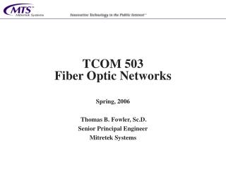
TCOM 503 Fiber Optic Networks. Spring, 2006 Thomas B. Fowler, Sc.D. Senior Principal Engineer Mitretek Systems. Topics for TCOM 503. Week 1: Overview of fiber optic communications Week 2: Brief discussion of physics behind fiber optics Week 3: Light sources for fiber optic networks

E N D
TCOM 503Fiber Optic Networks Spring, 2006 Thomas B. Fowler, Sc.D. Senior Principal Engineer Mitretek Systems
Topics for TCOM 503 • Week 1: Overview of fiber optic communications • Week 2: Brief discussion of physics behind fiber optics • Week 3: Light sources for fiber optic networks • Week 4: Fiber optic components fabrication and use • Week 5: Modulation of light, its use to transmit information • Week 6: Noise and detection • Week 7: Optical fiber fabrication and testing of components
Week 3: Light sources and propagation of light in fibers • Overview of light production • Physical background for lasers and LEDs • Construction and operation of LEDs • Characteristics and uses of LEDs in fiber optics • Principle of the laser • Types of lasers and their characteristics and uses • Semiconductor lasers for fiber optics
Light production • Basic principle: Rapid change of state of an electron • Must go from high energy state to lower energy state • Loss of energy must appear somewhere • Emitted in form of light • Lattice vibrations • Electron can be bound to a particular atom or molecule or be free (part of electron “gas”), as in most conductors • Two types of emission of light • Spontaneous • Stimulated
Light production: spontaneous • Normal case • Electron in high energy state is unstable • Spontaneously returns to lower state • Occurs in a few picoseconds • Photon emitted in process • Direction, phase random • Energy of photon determined by transition undergone by electron
Energy bands and light production 3p Energy levels split into bands overlap 3s 2p Electrons dropping and giving off light 2s 1s
Light production: stimulated • Electron in high energy metastable state • Can remain there for a “long” time (~microseconds) • Can fall back spontaneously, or be “stimulated” to emit its energy by another photon • Incident photon must have correct energy • Newly emitted photon will have same wavelength, phase, and direction as incident (stimulating) photon
Sources of energy for photon emission • Heat • Electrical discharge • Electric current • Chemical reaction • Biochemical reaction • Absorption of light • Nuclear radiation
Sources of energy: heat • Most common way of providing energy to boost electrons into higher energy states • Electrons may go to multiple states and then fall back • Depending on nature of heating process, result may be either “black body” radiation, or emission of energy at specific wavelengths characteristic of the material • Black body radiation is at all wavelengths, with distribution a function of temperature but not material • Characteristic of incandescent light bulbs
Sources of energy: electrical discharge • Electric current passed through gas • Energy from current ionizes gas • Breaks chemical bonds • Energizes electrons in gas • When they rejoin molecules, energy emitted in form of light • Called “florescence” • Principle of florescent lights • Photons emitted at specific wavelengths, but at random times, with random phases • Specific wavelengths easily seen with spectroscope
Sources of energy: electric current • Electric current applied to semiconductor p-n junction • Requires combination of electrons and holes for current to flow • Electrons go from high energy conduction band to lower energy valence band • Yields either spontaneous emission or stimulated (laser) emission, depending on device fabrication
Sources of energy: chemical reactions • Some chemical reactions give off light • Not always associated with heat, as in burning or explosions • Atoms, molecules restructured • Some electrons may be left in high energy states • Energy may be given off as light • At present, not a source of light for lasers
Sources of energy: biochemical reactions • Known as bioluminescence • Special type of chemical reactions which occur in living things • Operate by chemical reactions which leave electrons in high energy state • Result is spontaneous emission • No lasing action from animals known at present
Sources of energy: absorption of light • Substance absorbs light of one wavelength • Moves to higher energy (excited) state • Gives off light at different wavelength • Spontaneous • Florescent light bulbs • Light produced by discharge (in Ar gas) is UV • UV light absorbed by coating (phosphor) and reemitted as visible light • Stimulated • Ruby laser • Tube on outside provides energy to ruby crystal
Sources of energy: nuclear radiation • Ionization caused by a particles (Helium nuclei) • Electrons scattered, moved to high energy levels • Fall back may result in emission of light • Similar effect can be caused by high energy b particles (electrons) • g rays (high energy photons) can also scatter electrons and result in ionization
Types of spontaneous emission • Incandescent light: light produced through heating of material • “Black body” radiation • Fluorescent light: light produced through energy source other than heat • Ceases after energy source removed • Phosphorescent light: light produced through energy source other than heat • Continues after energy source removed
Construction and functioning of LEDs • LEDs: Light Emitting Diodes • Free electrons in conduction band recombine with holes • Enter lower energy valence band • Energy emitted in form of photon • Easy to calculate l of emitted light: hf = ephoton lf = c f = c/l hc/l = ephoton l =hc/ephoton h = Planck’s constant, 4.14 x 10⁻¹⁵ eV/s c = speed of light, 3 x 10⁸ m/sec
Practical considerations • Some energy possessed by electrons is in form of “lattice momentum” • Must be same in both conduction and valence bands • If not, some energy must be given up as a “phonon”, a quantum of energy in form of lattice vibration • Makes emission of photon unlikely • Impurity sites allow electrons to jump between bands without emitting photon • Common semiconductor materials such as silicon and germanium have this problem
Practical considerations (continued) • Common materials that can be used • Silicon • Germanium
Practical considerations (continued) • Easy to get light emitted, but hard to get it out of p-n junction and into a fiber • Must concentrate light production in a small (active) region • Must get enough power to active region in order to produce desired amount of light • Must be able to dissipate power
Double heterojunction Source: Dutton
Schematic of double heterojunction Source: Dutton
Actual devices Edge emitting LED Surface emitting LED Source: Dutton
Coupling to fiber Source: Dutton
Characteristics of LEDs • Low cost (compared to some lasers) • Use of lasers of type developed for CD players began in 1996 because cost is 1/10 that of LEDs • Low power (100 microwatts) • Some high power LEDs are now available (75 mw) • Relatively wide spectral width ~ 5% of wavelength, or 50-100 nm • Will cause problems with chromatic dispersion • Incoherent light • Not suitable for single mode fiber • Physics of device prevent extremely rapid modulation (switching on and off) • Limited to about 300 Mbps
Lasers: overview • LASER = Light Amplification by Stimulated Emission of Radiation • Best type of light for optical communications • Single (or rather narrow) wavelength • Coherent • Can be modulated precisely (~0.5 fsec or ~2,000 THz) • Can produce relatively high power, ~20 mw for communications lasers • Easily coupled into fiber (50-80%)
Lasers: overview (continued) • Disadvantages • Cost • Until recently, much more expensive than LEDs • Extremely high performance applications require extremely high stability • Thermal regulation to assure wavelength stability • P-n diode to measure power and adjust bias current • Most lasers are single frequency, and only available in a limited number of frequencies • Tunable lasers have recently become available • Range narrow • Slow to tune • Analog modulation not generally done but is feasible
Lasers: basic principles • Material capable of high energy metastable state and correct bandgaps • Stimulated emission • Mirrors to confine light • Population inversion
Stimulated emission Source: Dutton
Difference between stimulated and spontaneous emission • Emitted photons do not have same wavelength, phase, direction as exciting photons or other energy source • Direction, time of emission random • Many different wavelengths—black body radiation • No metastable states—photon emitted instantaneously Spontaneous emission Source: Dutton
Bandgaps and energy levels • Only certain materials are capable of lasing action • Electrons can only orbit in certain positions • Correspond to discrete energy levels • Can only change by gain or loss of fixed quanta of energy (multiples of Planck’s constant, k)
Bandgaps and energy levels (continued) • Atom has “ground state” and “excited” states, which refer to energy of electrons • In ground state, electrons are at their lowest permissible energy levels • Occur in what are often referred to as “shells” • Innermost shells have electrons tightly bound • Low energy states • Unavailable for bonding or conduction • Outermost shell called “valence” shell or band • Higher energy (more loosely bound) • Electrons can easily absorb energy and move to still higher energy bands • Chemical reactions involve valence band
Bandgaps and energy levels (continued) • In a solid, where atoms are bound together, situation is more complicated • Pauli exclusion principle prevents any two electrons from having exactly the same energy • Leads to “bands” rather than single values for energy • Structure of the bands determines nature of the material
Bandgaps Valence band: Conduction band: Conductor Insulator Semiconductor Large gap Overlap – no gap Small gap Source: Redrawn from Dutton
Bandgaps (continued) • Conductors: valence band and conduction band overlap • Situation in metals, where electrons exist as a “gas” • Large number of electrons available to conduct • Small applied voltage moves them • Impulses transmitted at about 2/3 c • Individual electrons travel very slowly (“drift velocity”)
Bandgaps (continued) • Insulators: large energy gap between conduction and valence bands • Large amount of applied energy needed to move an electron into conduction band • Can happen occasionally through thermal effects, etc. • Few electrons available unless applied electric field extremely large ~ 1000s of volts (insulator “breaks down”) • Typical of non-metals
Bandgaps (continued) • Semiconductors: Valence and conduction bands very close • Only small amount of energy needed to promote electron to conduction band • Between metals and non-metals
Semiconductors - elements Source: Lawrence Livermore Labs
Semiconductors: silicon • Lattice structure • Pure crystal near absolute 0 (-273.15o C) has no free electrons, cannot conduct • At room temperature, some electrons in conduction band due to thermal energy • As group IV element, silicon has 4 valence electrons Source: Dutton
Semiconductors—doping • To control properties of semiconductors, and get useful materials, necessary to add impurities • Called “dopants” • Added in very controlled manner to extremely pure silicon (or other material) • Typically 1 atom of dopant per 108 atoms of Si • Boron atom substituted for silicon atom in lattice • 3 electrons in valence band, leaves deficit in lattice, known as “hole” • Called “p-type”, where p comes from “positive” • Phosphorus atom substituted for silicon atom in lattice • 5 electrons in valence band, surplus in lattice, known as “free electron” • Called “n-type”, where n comes from “negative”
Semiconductors—p-type, n-type Source: Dutton
Properties of p-type, n-type semiconductors • Both conduct electricity, but not as well as conductors • N-type contains free and mobile electrons • P-type holes act as positive particles • Move much slower than electrons • In reality, bound electrons migrate in opposite direction, but visualization of holes moving is accurate • Electricity travels much slower in p-type material • Lattice with holes can exist next to lattice with free electrons • Little interaction • Holes, electrons combine at boundary • Release of energy can yield photon
p-n junctions: no applied voltage • Electrons diffuse from n-type region, holes from p-type region • Combine in middle to form “depletion zone” • Leaves net negative charge in p-type region and net positive charge in n-type region • Inhibits further crossing and recombining Source: Dutton