RANGAKAIAN DIODA
RANGAKAIAN DIODA. Hamzah Afandi, Antonius Irianto dan Betty Savitri Sources: Millman, Jacob, Grabel, Arvin, Microelectronics, Mc. Graw Hill Int. Ed., 1994. Robert Boylestad, Louis Nashelsky Sixth Edition; Prentice Hall,1997. Review: p-n Junction Volt-Ampere Characteristic of Diode.


RANGAKAIAN DIODA
E N D
Presentation Transcript
RANGAKAIAN DIODA Hamzah Afandi, Antonius Irianto dan Betty Savitri Sources: Millman, Jacob, Grabel, Arvin, Microelectronics, Mc. Graw Hill Int. Ed., 1994. Robert Boylestad, Louis Nashelsky Sixth Edition; Prentice Hall,1997
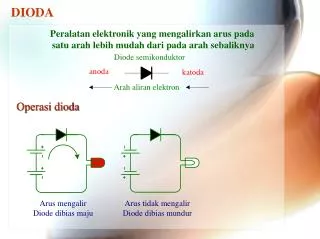
Review: p-n JunctionVolt-Ampere Characteristic of Diode = type of semiconductor factor ( for Si = 2, Ge = 1 ) VT = Volt-Equivalent of Temperature = 25 mV (at 293 oK) ID VZ IS VD V (0.6 - 0.7 for Si) (0.2 - 0.3 for Ge)
R VAA + R VD ID _ Quiscent Point IDQ VD VDQ VAA Review: p-n JunctionLoad-line Concept + ID VAA _
ID _ + VD K K K K K A A A A A Analysis of Diode Circuit:Ideal Diode Approach Reverse ID Forward/Active VD
Diode Circuit: +5V +9V 1K 10K 10K 1K -5V -9V Simple diode circuit analysis (d) (c) (a) (b)
Diode Circuit: Simple diode circuit analysis +10V Q: V12 = ….. ? (D = ON/OFF ?) Assumption that Diode is OFF R3 R1 4K 2K V1 V2 D R4 6K 2K R2 Diode is CORRECTLY OFF!
Diode Circuit: 0V A LOGIC GATE VI VO +5V +6V +5V 0V 0V RS +6V VI VO D1 RL
Diode Circuit: +6V VA VB +6V A LOGIC GATE VB VA VO +5V +6V +6V +5V 0V +6V 0V +6V 0V 0V RS 0V 0V 0V D1 VO RL D2 It's an 2 inputs AND-GATE! (Hey....How about 5 inputs?)
Diode Circuit: Vi Vo 20V + 20V 10V Clipping Circuit R1 D 10V
Diode Circuit: Vi Vo 20V 20V -10V Clipping Circuit R1 D + 10V
Diode Circuit: Vi Vo 20V 20V 10V -10V Clipping Circuit R1 D1 D2 + 10V 10V
Diode Circuit: Diodes as Rectifiers (Half Wave Rect.) Vo D RL
Diode Circuit: Diodes as Rectifiers (Full Wave Rect.) D1 Vo RL D2
Diode Circuit: Diodes as Rectifiers (Full Wave Rect.) Vo D1 D2 D3 D4 RL
Diode Circuit: C Diodes as Rectifiers (Full Wave Rect. + Filter) Vo D1 D2 D3 D4 RL
Diode Circuit: Diodes as Rectifiers (Voltage Regulator Concept) Vr = Ripple Voltage (RMS),VDC = DC Output Voltage VNL = DC Voltage at no-load VFL = DC Voltage at full-load
Diode Circuit: Vi Peak Detectors D C R VO
Diode Circuit: D C R Vi AM Demodulator Vo
Diode Circuit: Vi VSP + Voltage Doubler 2V SP _ + VO = 2 VSP D2 C1 + D1 _ C2
Diode Circuit: +Vs +Vs i + i = 0 _ VC v v _ + t Switching Flyback +Vs L L L VSW D + _ SW SW SW C t
Diode Circuit: +Vs i + _ Flyback Prevention +Vs _ i L L D D + SW SW
ID=(VD-V )/RF 1/Rf VZ IS V 1/Rr ID=(VD/RR) - IS Analysis of Diode Circuits:Large-Signal Model (Piecewise Linear Approach) ID VD
Analysis of Diode Circuits:Large-Signal Model (Piecewise Linear) A A A A Rf Rr IS V K K K K K ID=(VD-V )/RF ID=(VD/RR) - IS Forward-Biased Diode (On) Reversed-Biased Diode (Off)
+ Analysis of Diode Circuits:Characteristic Transfer Curve Method R1 vo Vo D 20V 1/Rf 10V vi 10V 1/Rr Vi 20V
+ -10 10 Analysis of Diode Circuits:Using PWL & Characteristic Transfer Curve Solve For: vi D1 5K vO D2 t 5K 5V 5V
CALCULATIONEXAMPLES Given in class