Download
1 / 14
140 likes | 285 Views
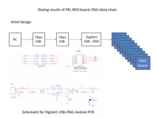
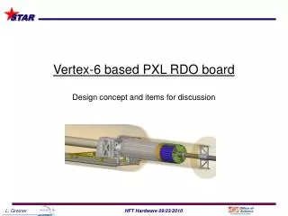
Vertex-6 based PXL RDO board Design concept and items for discussion. Outline. Current Xilinx Virtex-5 Design Proposed new Virtex-6 based design concept Outstanding questions and areas where clarification is needed. Current V-5 Design. SIU. TCD. USB. V-5 Dev board. Ladder 1. Ladder 3.

E N D
Vertex-6 based PXL RDO board Design concept and items for discussion
Outline • Current Xilinx Virtex-5 Design • Proposed new Virtex-6 based design concept • Outstanding questions and areas where clarification is needed.
Current V-5 Design SIU TCD USB V-5 Dev board Ladder 1 Ladder 3 Ladder 2 Ladder 4 SRAM Misc i/o ADC SRAM • Monolithic MB design. • All components are designed onto MB. • Design concept – do not load all functions onto production MBs.
Proposed V-6 based Design V-6 MB Expansion card TCD Ladder 1 SRAM USB ADC USB SRAM 240T V-6 Ladder 2 Advanced Header Interface Misc i/o Advanced Header Interface Ladder 3 SIU Ladder 4 SIU (shown with possible functionality) • Basic PXL RDO functionality with add-on cards for testing and i/o. • The V-6 MB contains all functionality for production PXL RDO. • Expansion card contains all other needed testing and non-baseline RDO functionality.
Comments and questions • The current data-rate bottleneck in the RDO system is the SIU. (we currently do meet the STAR requirements by a factor of >2 at 1kHz data rate) This gives us an option to add another SIU if needed. • This allows us to make the production RDO board as simple as possible but to preserve the needed functionality for testing. • There will be only minimal firmware modification needed (pin assignments which are needed for V-6 anyway. • Can we run the ADC (320 MHz interface) on a daughter-card? - yes • Do we want/need remote configuration? – yes via JTAG • We can use a linux friendly USB interface on the expansion card.
Proposal for the Physical Layout of PXL RDO motherboard L. Greiner 04/10/2011
Total panel IO connector space for production board • 4 x VHDCI 2 layer to maintain possible use with Phase-1, (http://www.molex.com/pdm_docs/sd/743370011_sd.pdf) We use 100 of the 136 pins arranged so that Ultimate sensor fits on a single cable. – 42.7mm x 12.77mm • 1 x SIU ~38mm • 1 x JTAG (daisy chain) ~22mm • 1 x TCD input (multi-drop) ~50mm • 1 x USB ~45mm • 1 x expansion card (room for USB + SIU + ADC inputs + misc i/o outputs on 3 x RJ-45) ~158mm Total panel space needed (can be front and back of boards) ~326mm + expansion board space
VHDCI connector (SCSI-5) 80MHz DDR (160 MHz effective data rate) Very robust connector and cable mating system
Proposal to use VME mechanical standard • VME crates exist and are a STAR standard. The components that we need can fit into a 9U VME form factor board (h)366.7mm x (d)340mm. • Our system consists of 10 RDO boards. Using double wide boards, this fits nicely into a 21 slot VME crate. • A P1 or P2 backplane can be used to distribute power and ground (our system uses +5V only). Which backplane we use depends on other factors such as if we wish to use any of the bussed signals on P1 (backplane specs here http://www.elma.com/Admin/ProductionFiles1//ProductTypeFile/24/English/VME_Reference_Sheet.pdf)
Some mechanical design adaptations • Our RDO PCBs are likely to be ~0.100” thick since they will be ~20 layer. The VME crate has card slots for standard 0.062” PCBs. • We can make a smaller PCB with mounting holes to allow the top and bottom of the PCB to be 0.062” and fit into the card slots (h)366.7mm x (d)340mm. VME card guide
Proposed RDO Board layout SIU VME P1 Expansion board TCD VHDCI JTAG USB
Can we use the P1 for TCD distribution? • We have a bussed backplane, why not use it for TCD distribution? • We can make a 6U card and do PECL to TTL conversion as well as the BUSY “OR” and install it in the 21st slot. VME Slot 1 VME backplane CLK, TRG word, etc. BUSY RDO Boards Disadvantages – somewhat harder to test and troubleshoot. Advantage – less connectors on front panel, true bus distribution.
Proposed 6U + 10 x 9U board RDO layout VME P1 TCD SIU Expansion board TCD 6U VME Board JTAG x10 USB
Testing and conclusions • We will do BER testing for VHDCI + commercial VHDCI cables as a function of length and frequency. A test plan can be found at http://rnc.lbl.gov/hft/hardware/docs/LVDS/VHDCI_and_cable_testing.docx • We will test the TCD signal transmission over VME P1 backplane (this is already working for the existing STAR TCD system) • This is the current PXL RDO motherboard design implementation of choice.