Sensor (0,0)
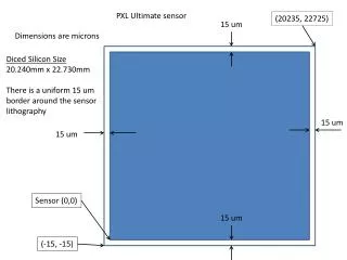
PXL Ultimate sensor. (20235, 22725). 15 um. Dimensions are microns. Diced Silicon Size 20.240mm x 22.730mm There is a uniform 15 um border around the sensor lithography. 15 um. 15 um. Sensor (0,0). 15 um. (-15, -15). Optical fiducial point locations are shown on the next pages.

Sensor (0,0)
E N D
Presentation Transcript
PXL Ultimate sensor (20235, 22725) 15 um Dimensions are microns Diced Silicon Size 20.240mm x 22.730mm There is a uniform 15 um border around the sensor lithography 15 um 15 um Sensor (0,0) 15 um (-15, -15)
Left side Right side
Right Side This corner X= 18165.075 µm Y= 871.6 µm
Left Side This corner X= 4594.225 µm Y= 920.775 µm
Ladder end detail Sensors are aligned to the upper edge of the cable 3.1 mm
214.48 mm 91.02 mm Driver section Low mass sensor section 1 mm gap Total length = 306.5 mm Width = 24.43 mm
Joe Silber - Attached are measurements I made yesterday. 1) If I divide the total width of 10 butted sensors by 10x Leo's nominal width (19.62mm) I get an average gap of 2um. 2) If I instead divide by the width I measured (19.607mm) then I get average gap of 16um. 3) If I add up the worst cases of offset and rotation that I measured, then the maximum tol envelope would be 54um. 4) If I add up the stdevs on offset and rotation that I measured, then the tol envelope should be 18um. Clearly I may be simply interpreting the edge of sensor incorrectly due to my lighting conditions. If so, then the average gap is is tiny, 2um, as in case (1). But if I am seeing things correctly on the smartscope, then this batch of sensors were cut undersized by about 13um on average, and the correct gap to model would be more like 16-18um, as in cases (2) and (4). Case (3) is essentially what Howard originally assumed (2 mil), but in reality it looks to me like it would be incorrect for us to assume this worst-case placement on every sensor. I think the bottom line is that if Leo can stomach about 100um maximum error for wire bond alignment, then we should be fine splitting the difference between the 2 um and 18 um numbers, and calling the nominal gap 10um.
Gap detail 10 um
ULTIMATERun SA35C11_1 # 12404 CC - IPHC 8th March 2011 - ULTIMATE
Traceability – Chip Numbering CC - IPHC 8th March 2011 - ULTIMATE
Sawing Diagram CC - IPHC 8th March 2011 - ULTIMATE