Download
1 / 1
40 likes | 258 Views
Microlens Array Light Trapping CdTe Solar Cells for use in Concentrator Photovoltaics. Student : Patrick Margavio , Mechanical and Aerospace Engineering. Faculty Advisor : Dr. Hailung Tsai, Mechanical and Aerospace Engineering. What is Light Trapping?

E N D
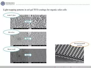
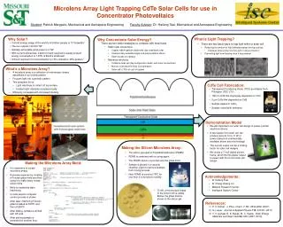
Microlens Array Light Trapping CdTe Solar Cells for use in Concentrator Photovoltaics Student: Patrick Margavio, Mechanical and Aerospace Engineering Faculty Advisor: Dr. Hailung Tsai, Mechanical and Aerospace Engineering • What is Light Trapping? • There are two basic ways to trap light within a solar cell • Reducing the amount of light reflected away from top surface • Examples below scatter incoming light to reduce reflection3 • Preventing light from leaving once it has entered • Why Concentrate Solar Energy? • There are two basic strategies to compete with fossil fuels • Make solar inexpensive • Copper indium gallium diselenide, dye sensitized solar • Commercially available single and polycrystalline silicon • Solar houses on campus • Maximize efficiency • Combine solar cell (like multijunction GaAs) with solar concentrator • Mirrors, Luminescent Solar Concentrators • Solar cell is 75% of cost of system • Why Solar? • Current energy usage of the world’s 6.5 billion people is 13 Terawatts1 • The sun outputs 120,000 TW • Globally extractable wind power is 4 TW • With current efficiencies, fraction of land required to supply present energy consumption is 1.35% of Earth’s landmass2 • Amount required for food production is 13% cultivation, 26% pasture2 • What’s a Microlens Array? • A microlens array is a collection of microscopic lenses assembled in an orderly pattern • Focuses light into a periodic pattern • Two purposes for us • Light less likely to reflect off top surface • Incident light intensity increased locally • Efficiency increases with increased intensity • Making the Silicon Microlens Array: • The silicon gel used is Polydimethylsiloxane (PDMS) • PDMS is combined with a curing agent • The PDMS mixture is poured over the glass mold • Sample is placed in a vacuum chamber (right) to remove bubbles from mixing process • Next PDMS is cured at 700C for one hour in a furnace to solidify • Acknowledgements: • Dr Hailung Tsai • Dr Cheng-Hsiang Lin • Material Research Center • Intelligent System Center • References: • P. V. Kamat. J. Phys. Chem. C 111, 2834-2860 (2007) • A. Luque. Journal of Applied Physics 110, 031301 (2011) • V. V. Iyengar, B. K. Nayak, M. C. Gupta. Solar Energy Materials and Solar Cells 94, 2251-2257 (2010) • CdTe Cell Fabrication: • Transparent Conducing Oxide (TCO) purchased from Pilkington (TEC C10) • 150 nm CdS film chemically deposited on TCO • 5 µm CdTe film deposited on CdS • Sample dipped in CdCl2 • Sample rinsed with methanol • Demonstration Model • We will implement our solar cell design to power a small electronic device • A two square inch solar cell can produce around 10 to 11 W of power (based on commercially available silicon solar technology) • The current output can be a limiting factor for solar cell designs • We chose a 7 inch digital picture frame, which fits this power outputto power with the 2 inch solar cell design • It is expensive to create microlens arrays • Decrease expense by creating a Foturan glass mold and then using it to make many cheap silicon films • Mold is created by laser machining • G code used to computer control process is shown • After laser machining Foturan glass is baked at 5000C and then at 6000C. • After baking, sample is etched with HF acid • After etching sample is annealed for another hour Making the Microlens Array Mold: • To left, a microscope image of the silicon film is visible. Below, the glass mold is shown in the silicon gel