Download
1 / 19
210 likes | 456 Views
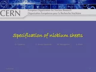
ECR Deposition of Niobium. ECR plasma principle Cavity deposition system prototype Surface treatment NbN surface coating. A-M. Valente, L. Phillips, H. Wang, A. Wu, R. Bundy, T. Goodman, R. Rimmer, C. Reece, Jefferson Lab G. Wu , Fermilab H. Padamsee, Cornell University.

E N D
ECR Deposition of Niobium • ECR plasma principle • Cavity deposition system prototype • Surface treatment • NbN surface coating A-M. Valente, L. Phillips, H. Wang, A. Wu, R. Bundy, T. Goodman, R. Rimmer, C. Reece, Jefferson Lab G. Wu, Fermilab H. Padamsee, Cornell University Thin Films and new ideas forpushing the limits of RF superconductivity
Illustration of the energetic vacuum deposition by ECR plasma Wu, G., et al., J. Vac. Sci. Technol. A Vol. 21, No. 4, (2003) Thin Films and new ideas forpushing the limits of RF superconductivity
Thin Films and new ideas forpushing the limits of RF superconductivity
Total ionization cross section of 5 outer shell electrons Right electron kinetic energy Off-resonant ECR to achieve longer electron life and right ionization energy Thin Films and new ideas forpushing the limits of RF superconductivity
Niobium Plasma Ion Energy Distribution measured by the Analyzer Thin Films and new ideas forpushing the limits of RF superconductivity
ECR cavity deposition system • 14kW rod-fed E-gun • 9000 l/s cryopump system • bucking coil for E-gun • top and bottom iron yokes (outer iron shield is removed for illustration) • center coils • Nb grid tube • bias insulator • WR284 waveguide E-bend and horn to the grid tube • “T” vacuum chamber • top pancake coil • Cu cavity • bottom pancake coil. Potential use for surface cleaning and Nb3Sn, NbN coatings Thin Films and new ideas forpushing the limits of RF superconductivity
Large volume of ECR magnetic field Sample deposition system 7.5kW hearth, 130 A/s Cavity deposition system 15 kW Rod-fed, 100 A/s Magnetic field Slight radial confinement Thin Films and new ideas forpushing the limits of RF superconductivity
Inside E-gun chamber Thin Films and new ideas forpushing the limits of RF superconductivity
Thin Films and new ideas forpushing the limits of RF superconductivity
147/250W RF Ar: 1.2e-5 Torr 238/250W RF Ar: 2.9e-5 Torr (230-260)W/293 W Nb: ~3.5 kW Ar: 15.7 eV Nb: 7.0 eV Thin Films and new ideas forpushing the limits of RF superconductivity
Summary of thin film sample • Niobium Ion Energy is around 63 eV without bias voltage, and controllable. • Cryogenically, the process achieves a reasonably high RRR niobium thin film with excellent superconducting transition temperature and width. • RRR appears to be more closely related to the film thickness than to the deposition energy. • Epitaxial growth of niobium on sapphire has been achieved. The substrate bias voltage of -60 V is believed to be the preferred value based on the transition width, the crystal orientation spread, and the AFM results. • For a copper substrate, a better film quality likely requires higher deposition energy than sapphire substrate, which needs further studies. • Nb-Cu sample surfaces are smooth locally • Nb-Cu surfaces may have much less hydrocarbons and other residuals or contaminants as compared with those on the Nb surfaces obtained conventionally (BCP or EP). • Nb-Cu samples appear to have more oxygen on the surfaces and oxygen penetrates deeper into the interior of the samples. This may be resulted from the residual gases in the deposition chamber and from the fact that the grain size of Nb-Cu is small. Thin Films and new ideas forpushing the limits of RF superconductivity
A multilayer sample of Nb-NbOx-Nb • Copper substrate was prepared by electropolishing. • First layer of Nb was deposited at 500 V bias voltage. • Exposed to air to form Nb oxides. • Second layer (thicker) of Nb was deposited at 60 V bias voltage. • TEM sample prepared (FIB) and analyzed at SANDIA TEM by T. Renk, P. Provencio, SNL Thin Films and new ideas forpushing the limits of RF superconductivity
Nb Cu substrate 3-5 nm Nb oxides 10 nm Nb Thin Films and new ideas forpushing the limits of RF superconductivity
Plasma surface treatment • Surface smoothening through coating Potential cross the surface by ASE/Dacapo Use (NEB) method to find energy barriers for various diffusion processes on the surface. MD for lattice dynamics KMC/MD combination to simulate the film growth J. Pomeroy, Ph.D Dissertation, Cornell University Thin Films and new ideas forpushing the limits of RF superconductivity
RMS = 1274 nm BCP RMS = 94 nm Nb/Cu RMS = 251 nm EP RMS = 35 nm BEP A. Wu, Jlab Thin Films and new ideas forpushing the limits of RF superconductivity
Alternative processes for bulk niobium cavity treatment Degrease or light etching After RF tuning, prepare a UHV degrease Water rinsing Light water rinsing or ultrasonic water rinsing De-oxidation High impact energy Ar ion pre-etching of the cavity 1,000 nm smooth coating ECR deposition of a smoothening high purity Nb layer 2 hour 800 C bake to decrease the hydrogen content and moderate re-crystallization 800 C bake HPW rinsing High pressure water rinsing before final assembly Thin Films and new ideas forpushing the limits of RF superconductivity
Some mosaicity is inevitable in film. That is less detrimental than grain boundary, yet prone to deep oxidation and possible RF dissipation. G. Wu, et al., Thin Solid Film, Vol 489/1-2 pp 56-62, 2005 A. Wu, et al., PAC05, Knoxville, TN, 2005 O. Hellwig, Ph.D dissertation, Ruhr-Universität Bochum, 2000 Thin Films and new ideas forpushing the limits of RF superconductivity
NbN by plasma injection? • ECR plasma of Nitrogen can be achieved at low pressure, N+ can travel to the substrate without much energy loss • Bias voltage can be reversed to stop ion impact immediately (To lessen the metallic Nb2N forming) • Bias voltage could potentially be adjusted for proper phase control: -NbN or Nb3N4 (insulator) Thin Films and new ideas forpushing the limits of RF superconductivity
Acknoledgement JLAB ECR thin film collaboration: Cornell: H. Padamsee (LEPP), L. Hand (Physics) College of William and Mary: M. Kelley SANDIA: T. Renk, P. Provencio Black Laboratory: R. Crooks LANL: T. Tajima Thin Films and new ideas forpushing the limits of RF superconductivity