High Frequency Design & Measurement
10 likes | 172 Views
High Frequency Design & Measurement Dr. Branimir Pejcinovic, Dr. Melissa Holtzman and Betsy Natter. Microelectronics, Nanoelectronics and Electromagnetics

High Frequency Design & Measurement
E N D
Presentation Transcript
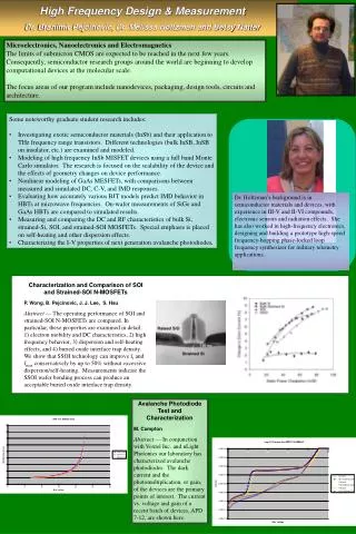
High Frequency Design & Measurement Dr. Branimir Pejcinovic, Dr. Melissa Holtzman and Betsy Natter Microelectronics, Nanoelectronics and Electromagnetics The limits of submicron CMOS are expected to be reached in the next few years. Consequently, semiconductor research groups around the world are beginning to develop computational devices at the molecular scale. The focus areas of our program include nanodevices, packaging, design tools, circuits and architecture. • Some noteworthy graduate student research includes: • Investigating exotic semiconductor materials (InSb) and their application to THz frequency range transistors. Different technologies (bulk InSB, InSB on insulator, etc.) are examined and modeled. • Modeling of high frequency InSb MISFET devices using a full band Monte Carlo simulator. The research is focused on the scalability of the device and the effects of geometry changes on device performance. • Nonlinear modeling of GaAs MESFETs, with comparisons between measured and simulated DC, C-V, and IMD responses. • Evaluating how accurately various BJT models predict IMD behavior in HBTs at microwave frequencies. On-wafer measurements of SiGe and GaAs HBTs are compared to simulated results. • Measuring and comparing the DC and RF characteristics of bulk Si, strained-Si, SOI, and strained-SOI MOSFETs. Special emphasis is placed on self-heating and other dispersion effects. • Characterizing the I-V properties of next generation avalanche photodiodes. Dr. Holtzman’s background is in semiconductor materials and devices, with experience in III-V and II-VI compounds, electronic sensors and radiation effects. She has also worked in high-frequency electronics, designing and building a prototype high-speed frequency-hopping phase-locked loop frequency synthesizer for military telemetry applications. Characterization and Comparison of SOI and Strained-SOI N-MOSFETs P. Wong, B. Pejcinovic, J. J. Lee, S. Hsu Abstract — The operating performance of SOI and strained-SOI N-MOSFETs are compared. In particular, these properties are examined in detail: 1) electron mobility and DC characteristics, 2) high frequency behavior, 3) dispersion and self-heating effects, and 4) buried oxide interface trap density. We show that SSOI technology can improve ft and fmax conservatively by up to 50% without excessive dispersion/self-heating. Measurements indicate the SSOI wafer bonding process can produce an acceptable buried oxide interface trap density. Avalanche Photodiode Test and Characterization M. Compton Abstract — In conjunction with Voxtel Inc. and nLight Photonics our laboratory has characterized avalanche photodiodes. The dark current and the photomultiplication, or gain, of the devices are the primary points of interest. The current vs. voltage and gain of a recent batch of devices, APD 7-12, are shown here.